Silicon-based hybrid integrated laser array and preparation method thereof

A technology of laser array and hybrid integration, applied in the field of lasers, can solve the problems of device influence without research on heat dissipation characteristics of buried oxide layer and high epitaxy technology, and achieve the effect of improving heat dissipation characteristics and optoelectronic characteristics, simple and stable process, and stable process.

Active Publication Date: 2019-04-02
INST OF SEMICONDUCTORS - CHINESE ACAD OF SCI
View PDF11 Cites 17 Cited by
  • Summary
  • Abstract
  • Description
  • Claims
  • Application Information

AI Technical Summary

Problems solved by technology

Although this solution can realize self-aligned silicon-based hybrid integrated lasers on an SOI material, it does not require precise alignment technology between SOI and III-V, but the requirements for epitaxy technology are very high, and the current technology is still immature. It needs to be explored, and the influence of poor heat dissipation characteristics of the buried oxide layer in the SOI substrate on the device has not been studied

Method used


Image

  • Silicon-based hybrid integrated laser array and preparation method thereof
  • Silicon-based hybrid integrated laser array and preparation method thereof
  • Silicon-based hybrid integrated laser array and preparation method thereof

Examples


Embodiment Construction

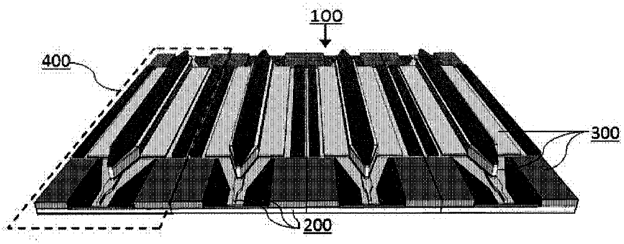
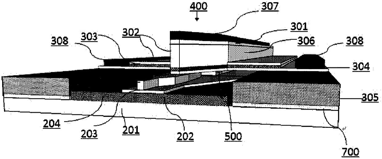
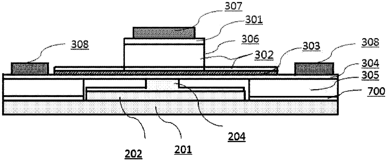
[0037]The disclosure provides a silicon-based hybrid integrated laser array and its preparation method, which has good heat dissipation characteristics and photoelectric characteristics, and the III-V semiconductor epitaxial material is epitaxially formed by MBE or MOCVD in one time, without the need for secondary epitaxy and selective growth technology, the process is simple and stable; the structure on SOI can be compatible with the mature CMOS process, the process is stable, the repeatability is good, and the production cost is low; the structure on the III-V semiconductor material can be compatible with the traditional optoelectronic process technology, and the production has High repeatability.

[0038] In order to make the purpose, technical solutions and advantages of the present disclosure clearer, the present disclosure will be further described in detail below in conjunction with specific embodiments and with reference to the accompanying drawings.

[0039] In a firs...


PUM


Abstract

The invention discloses a silicon-based hybrid integrated laser array and a preparation method thereof. The silicon-based hybrid integrated laser array comprises a plurality of distributed silicon-based hybrid integrated lasers in parallel integrated on an SOI substrate and an III-V semiconductor epitaxial layer. Each silicon-based hybrid integrated laser comprises: a silicon ridge waveguide; heatconducting layers located in special areas at two sides of the silicon ridge waveguide, wherein the special area is an area obtained after the SOI substrate removes a top silicon and a buried oxide layer; an intrinsic layer in a shape of a saddle and comprising a protrusion portion and a connection portion at two ends, wherein the protrusion portion at one end covers the upper portion of the heatconducting layers, the connection portion of the intrinsic layer is provided with an N-type waveguide layer, an active region and a P-type cover layer in order; an III-V waveguide formed by patterning the III-V semiconductor epitaxial layer and connected with the silicon ridge waveguide; a P-type ohmic contact layer; a P electrode; and an N electrode. The silicon-based hybrid integrated laser array is good in heat dissipation, simple and stable in preparation process, good in repeatability and low in manufacturing cost.

Description

Technical field [0001] The present disclosure belongs to the field of laser technology and relates to a silicon-based hybrid integrated laser array and a preparation method thereof. Background technique [0002] With the development of technology, people have higher and higher requirements for data transmission rate, transmission bandwidth and energy consumption. Restricted by the physical characteristics of electronics, traditional electrical interconnections based on electrical integrated chips consume energy when transmitting high-speed signals. Large, narrow bandwidth and high cost bottlenecks of optoelectronic integrated systems; photons have the characteristics of ultra-high transmission speed, ultra-high parallelism, ultra-high bandwidth and ultra-low transmission and interaction power consumption. Because silicon photonics integration combines the ultra-large-scale logic, ultra-high-precision manufacturing, and low-cost advantages of the CMOS process, silicon-based o...

Claims


Application Information

Patent Timeline
Patent Type & Authority Applications(China)
IPC IPC(8): H01S5/40H01S5/22H01S5/32
CPCH01S5/22H01S5/32H01S5/4025
Inventor 郑婉华王海玲王明金石涛孟然哲
Owner INST OF SEMICONDUCTORS - CHINESE ACAD OF SCI
Why Eureka
Try Eureka