Full-medium metasurface refractive index sensor based on polarization insensitive Fano resonance
A refractive index sensor, polarization-insensitive technology, applied in the direction of phase influence characteristic measurement, etc., can solve the problems of lossy price, inconvenient measurement, expensive, etc., and achieve the effect of meeting measurement needs, high quality factor, and high sensitivity
- Summary
- Abstract
- Description
- Claims
- Application Information
AI Technical Summary
Problems solved by technology
Method used
Image
Examples
Embodiment 1
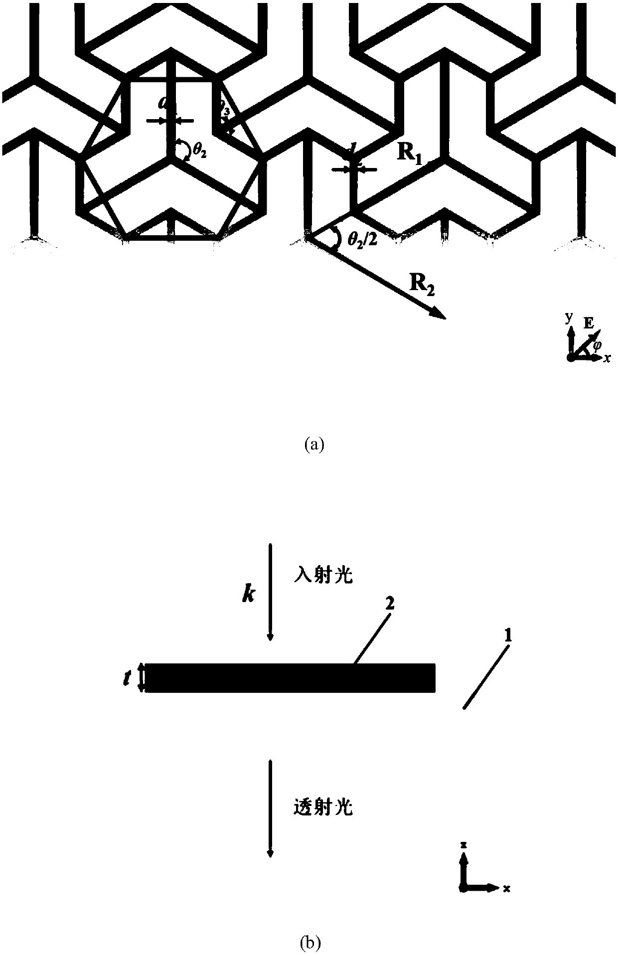
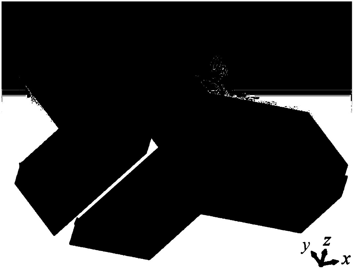
[0039] Based on the above-mentioned design principles, embodiments of the present invention provide an all-dielectric metasurface refractive index sensor based on polarization-insensitive Fano resonance, see figure 1 , the refractive index sensor consists of a dielectric substrate 1 and a dielectric metasurface microstructure unit array from bottom to top, the dielectric metasurface microstructure unit array is set on the dielectric substrate 1, and the dielectric metasurface microstructure unit array consists of several dielectric The composition of metasurface microstructure unit 2. Each dielectric metasurface microstructure unit 2 along R 1 and R 2 Periodically arranged in two directions.
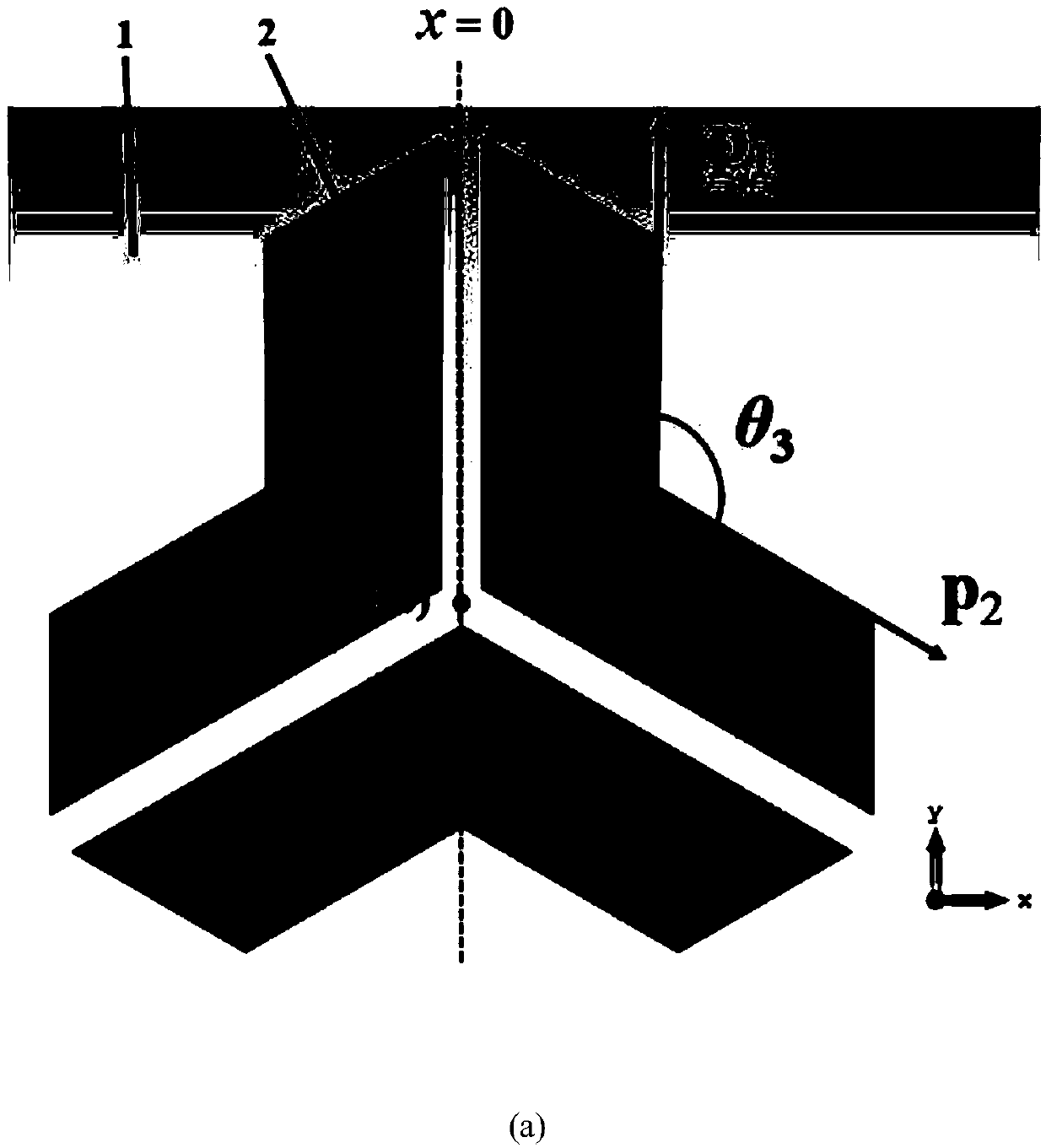
[0040] Among them, see figure 2 , each dielectric metasurface microstructure unit 2 is composed of three V-shaped dielectric antennas, the three V-shaped dielectric antennas are mirror-symmetrical about the x=0 plane and have 120-degree rotational symmetry, and the distance between t...
Embodiment 2
[0044]The scheme in Embodiment 1 is further introduced below in conjunction with specific device parameters, see the description below for details:
[0045] Wherein, the above-mentioned dielectric metasurface microstructure unit 2 is made of any one of single crystal silicon, polycrystalline silicon, silicon dioxide or titanium dioxide, and other dielectric materials. In actual implementation, this embodiment of the present invention does not limit it. The needs of the application are selected.
[0046] Furthermore, the thickness t of the dielectric metasurface microstructure unit 2 is preferably 5-200 nanometers, which is not limited in the embodiment of the present invention, and can be selected according to the needs of practical applications.
[0047] Preferably, the dielectric substrate 1 is made of any one of single crystal silicon, silicon dioxide or quartz glass; the materials of the dielectric substrate 1 and the dielectric metasurface microstructure unit 2 are differ...
Embodiment 3
[0054] Combine below image 3 , theoretically verify that the refractive index sensor provided by the embodiment of the present invention is not sensitive to the polarization state of incident light, see the following description for details:
[0055] Such as image 3 As shown, the dielectric metasurface microstructure unit 2 is mirror-symmetrical about the x=0 plane, and the plane wave is normally incident from top to bottom.
[0056] Assuming that the normal incident plane wave electric field is along the y-axis direction, the incident electric field is recorded as:
[0057] E. 0,i =C i y (1)
[0058] Among them, C i is a complex number, representing the complex amplitude value of the electric field along the y-direction component, and y is a unit length vector along the y-axis direction. Because the dielectric metasurface microstructure unit 2 is mirror-symmetric about the x=0 plane, according to the principle of electromagnetic field symmetry, it can be obtained by t...
PUM
| Property | Measurement | Unit |
|---|---|---|
| angle | aaaaa | aaaaa |
| thickness | aaaaa | aaaaa |
| refractive index | aaaaa | aaaaa |
Abstract
Description
Claims
Application Information


