Therefore, during the entire manufacturing process,
random defects and systematic defects may occur due to the accuracy deviation of the equipment itself, abnormal faults, particles produced by the process, drawing defects in the design
layout diagram and insufficient yellow light
process window (window) ( Random and systematic defect), these defects cause product open circuit (open) or
short circuit (short) type failure, reduce
wafer yield
These
random defects and systematic defects, as the size of the semiconductor manufacturing process shrinks down, the number of defects also increases greatly due to the reduction in size, so that thousands or tens of thousands of defects can be obtained in each defect detection, due to the limitation of the
scanning electron microscope (
Scanning Electron Microscope, SEM) can only select dozens to hundreds of defects to take pictures by sampling, which greatly increases the difficulty of sampling defects that will actually cause open circuit or
short circuit failure, so it cannot be accurate and real-time Provide SEM photos of defects that cause yield loss to process engineers, and it is difficult to analyze the source of defects in the process based on the SEM photos of defects. Therefore, the effect of improving defect yield is not good, and the cost of semiconductor factories is increased.
[0003] In the practical operation of semiconductor factories (for example:
foundry,
Foundry), real-
time data analysis of defects and image
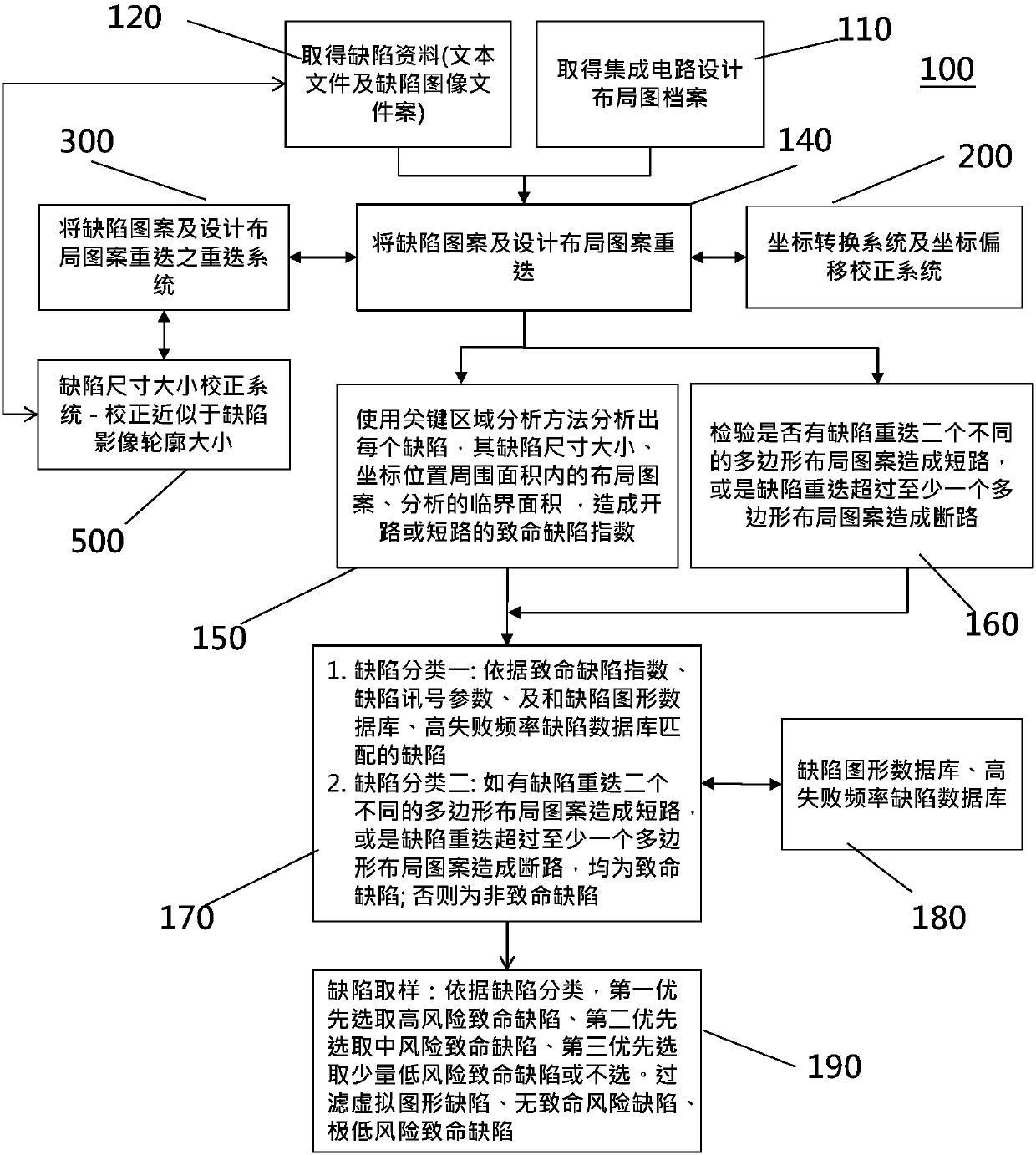
graphics classification was used to be an important method to improve yield in the past, but this method is not available in Nai It is difficult to find fatal defects in the defect analysis of the meter-level semiconductor manufacturing process; the core part of this innovation introduces IC design layout data, critical area analysis (Critical Area Analysis, CAA) method, defect pattern overlapping design layout, coordinates The conversion correction
system and the
defect size correction system are important breakthrough methods and systems to solve the fatal defects of sampling
[0004] Furthermore, the image profile measurement data of the SEM and
optical microscope and the defect data generated by the inspection
machine are compared with the key area
analysis data, and the
defect size and area data of the inspection
machine and the image profile of the SEM and
optical microscope are compared. There are differences in the measurement size and area data, resulting in differences in the analysis results of key areas. In order to solve the analysis deviation of key areas, the problem of
defect size deviation must be solved
For example: the defect
size measurement unit of the defect inspection
machine should be higher than the minimum size of the layout
graphics, resulting in a deviation between the size of the defect data and the actual defect size of the SEM photo
[0005] In addition, in the complex advanced process of miniaturized semiconductors, especially when the optical effect
process window (
process window) is getting narrower and narrower, but the IC design layout pattern is multiplied and complicated, resulting in some pattern-related defects being detected Out of them, the defects that will affect the
yield rate are "systematic defects", which will cause extremely low
yield rate, but if this graphic does not affect the IC design circuit, such as: monitoring
graphics, because it does not affect the
yield rate, that is It belongs to "false defect", but because the false defect pattern and
signal are obvious, it often accounts for most of the defect sampling rate to more than 90%, but it is impossible to really find the defect pattern of open circuit or short
circuit failure[0006] Finally, in the defect sampling part, in addition to the patent number US8312401B2 approved by the same inventor in 2012, the critical area
analysis method was used to obtain the key area of the design layout pattern within the defect size and coordinate deviation range of each defect, and calculated The probability value of open circuit or short-
circuit failure defects is the Killer Defect Index (KDI), which is the CAA value; however, when calculating the Killer Defect Index (KDI), the defect inspection machine is not loaded with the
wafer The precision of the control motor is taken into account, for example: when a defect inspection machine moves the
wafer, the coordinate accuracy unit is controlled as plus or minus W, for example, when W is equal to 0.05 microns, therefore, its detectable size is plus or minus 0.05 The multiple of microns; therefore, the
size value of the detected defect image may be larger than the actual size, which may cause problems such as a high fatal defect index

