Band-pass filter and preparation method thereof
A band-pass filter, channel technology, applied in waveguide-type devices, electrical components, circuits, etc., to achieve the effect of improving resonance frequency extraction, improving quality factor, and eliminating power consumption
- Summary
- Abstract
- Description
- Claims
- Application Information
AI Technical Summary
Problems solved by technology
Method used
Image

Examples
Embodiment 1
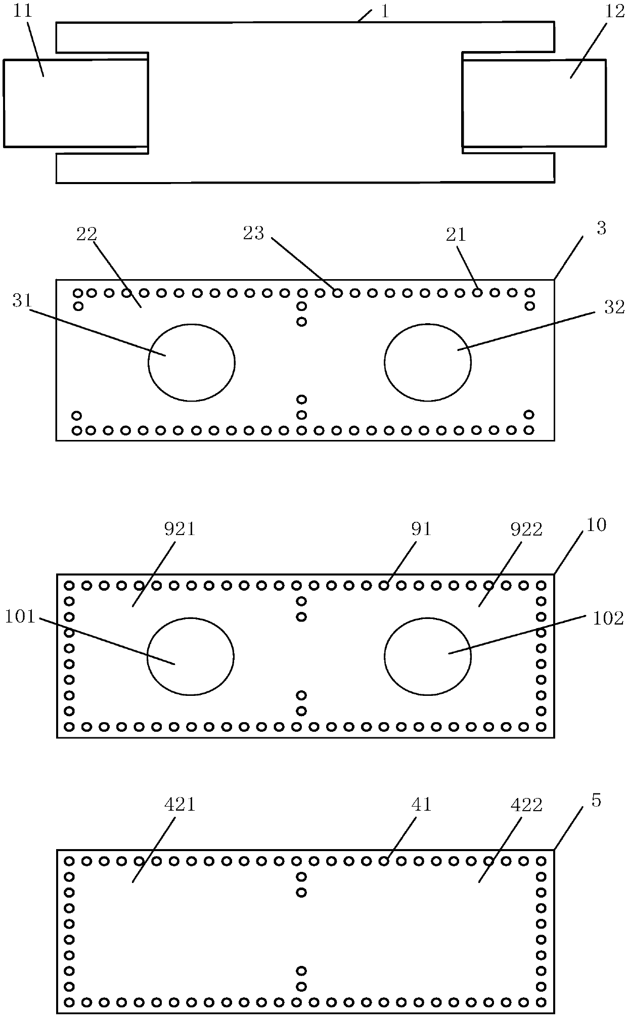
[0066] Such as figure 1 with figure 2 as shown, figure 1 It is a schematic diagram of a bandpass filter proposed by the present invention, figure 2 For the side view of the band-pass filter proposed by the present invention, this embodiment provides a band-pass filter, including:
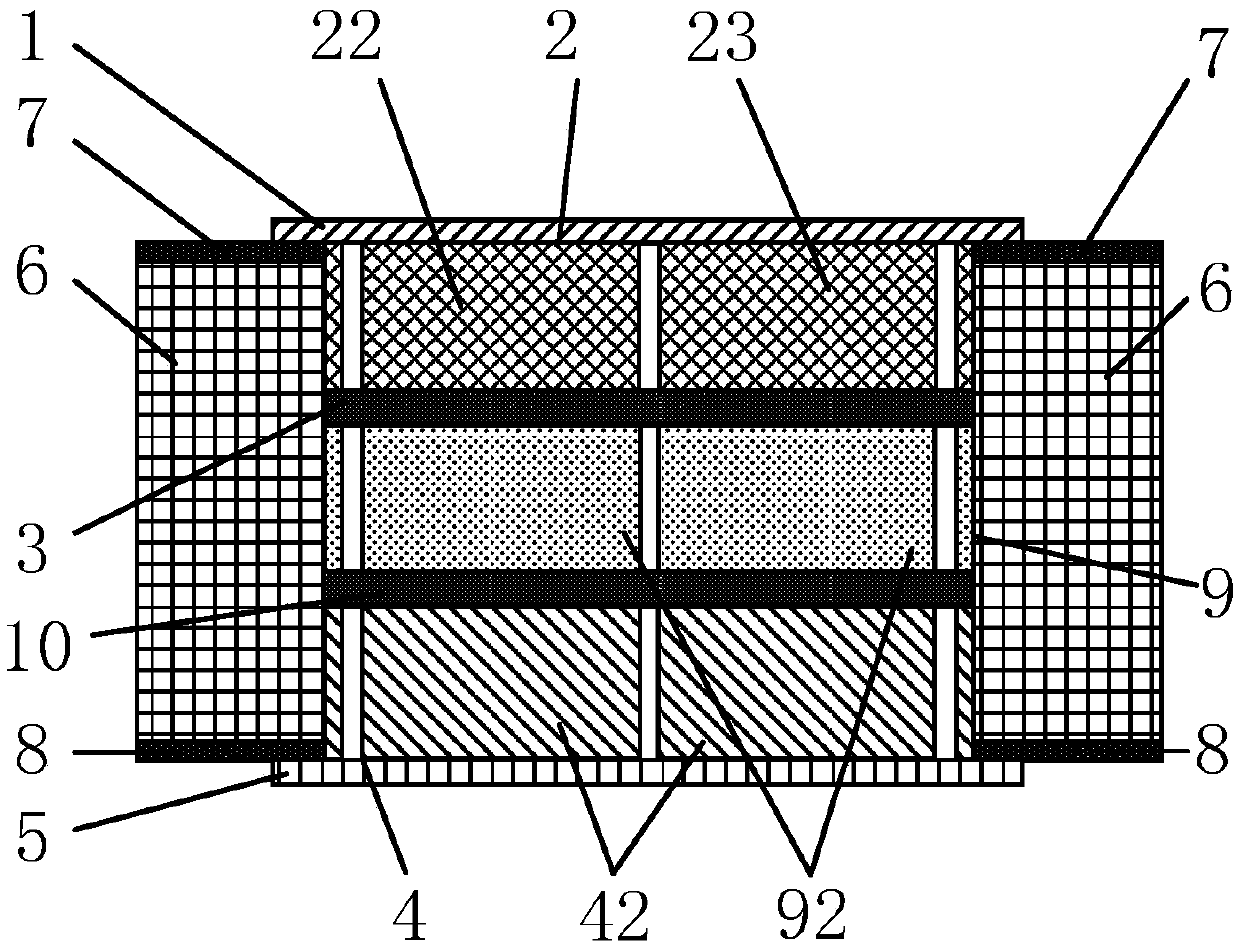
[0067] The ground layer 5, the top layer 1, and the upper dielectric cavity 2, the first window layer 3, the middle dielectric cavity 9, the second window layer 10 and the lower dielectric cavity 4 are sequentially arranged between the ground layer 5 and the top layer 1 from top to bottom, The upper dielectric cavity 2, the middle dielectric cavity 9 and the lower dielectric cavity 4 are made of air, which has a low dielectric constant, and the signal is transmitted in the air with almost no loss. The upper dielectric cavity 2, the middle dielectric cavity 9 and the The lower medium cavity 4 is designed with SIW structure, wherein,
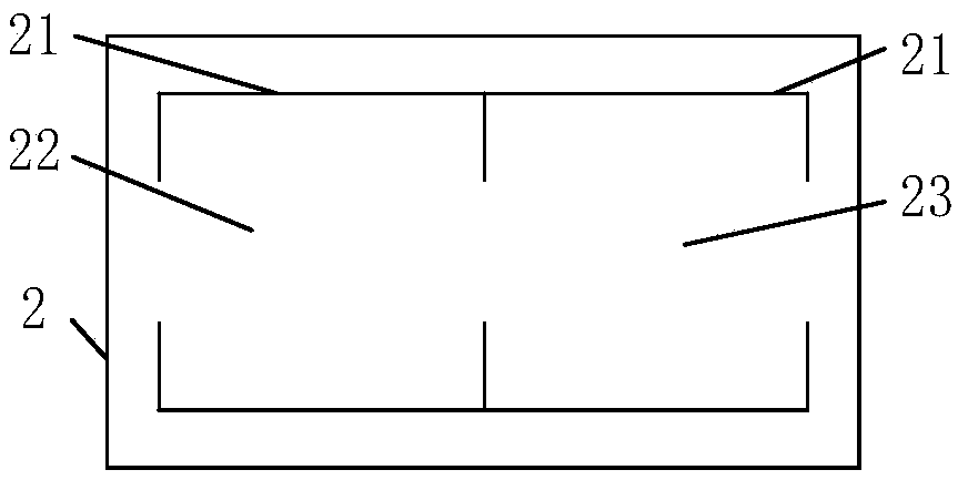
[0068] The upper dielectric cavity 2 is provided with a plur...
Embodiment 2
[0094] Such as Figure 5(a) ~ Figure 5(l) as shown, Figure 5(a) ~ Figure 5(l) It is a schematic flow chart of a method for preparing a band-pass filter proposed by the present invention. This embodiment provides a method for preparing a band-pass filter, including the following steps:
[0095] S01: Deposit an upper isolation layer 7 on the first surface of the silicon substrate 6, and form a top layer 1 on the upper isolation layer 7. The function of the production isolation layer is to prevent the top layer 1 from directly contacting the silicon substrate 6. The generated top layer 1 includes Input port 11 and output port 12, as shown in Figure 5 (a);
[0096] It should be noted that, after step S01 is completed, for the convenience of manufacturing, the top layer 1 is first bonded to the wafer 100, and the wafer 100 is used as a carrier and serves as the base part of the structure during the entire preparation process to prevent the top layer 1 from directly contacting the...
PUM
 Abstract
Description
Claims
Application Information
 - R&D
- Intellectual Property
- Life Sciences
- Materials
- Tech Scout
- Unparalleled Data Quality
- Higher Quality Content
- 60% Fewer Hallucinations
Browse by: Latest US Patents, China's latest patents, Technical Efficacy Thesaurus, Application Domain, Technology Topic, Popular Technical Reports.
© 2025 PatSnap. All rights reserved.Legal|Privacy policy|Modern Slavery Act Transparency Statement|Sitemap|About US| Contact US: help@patsnap.com