A kind of preparation method of silicon carbide single crystal thin film

A technology of silicon carbide single crystal and silicon carbide, which is applied in semiconductor/solid-state device manufacturing, semiconductor/solid-state device testing/measurement, electrical components, etc., and can solve problems such as difficult film and substrate separation and difficult application

Active Publication Date: 2021-03-09
UNIV OF SCI & TECH OF CHINA
View PDF5 Cites 0 Cited by
  • Summary
  • Abstract
  • Description
  • Claims
  • Application Information

AI Technical Summary

Problems solved by technology

Most applications of these methods almost require heteroepitaxially grown thin film samples. The heteroepitaxial growth technology of silicon carbide materials can only grow 3C silicon carbide thin films in the silicon [100] and silicon [111] crystal directions. However, the 4H silicon carbide high-purity thin film with spin color centers that has been studied more can only be obtained by homoepitaxial growth. The thin film material grown by homoepitaxial growth is difficult to realize the separation of the thin film and the substrate, and it is also difficult to realize the material in the photon Applications in crystals, surface plasmons, fiber optic cavities, and whispering gallery cavities

Method used


Image

  • A kind of preparation method of silicon carbide single crystal thin film
  • A kind of preparation method of silicon carbide single crystal thin film
  • A kind of preparation method of silicon carbide single crystal thin film

Examples


Embodiment Construction

[0029] The technical solutions in the embodiments of the present invention will be clearly and completely described below in conjunction with the accompanying drawings in the embodiments of the present invention. Obviously, the described embodiments are only some of the embodiments of the present invention, not all of them. Based on the embodiments of the present invention, all other embodiments obtained by persons of ordinary skill in the art without making creative efforts belong to the protection scope of the present invention.

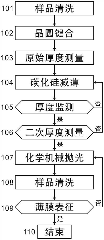
[0030] According to attached Figure 1-3 Shown, the present invention is further described:

[0031] figure 1 Provided as an embodiment of the present invention is a flow chart of a method for preparing a silicon carbide single crystal thin film. Such as figure 1 as shown,

[0032]The first step of the method for preparing a silicon carbide single crystal thin film is sample cleaning 101, which requires strict cleaning of the silicon carbide wa...


PUM


Abstract

The invention discloses a method for preparing a silicon carbide single crystal thin film. The technological process mainly includes: sample cleaning, wafer bonding, original thickness measurement, silicon carbide thinning, thickness monitoring, secondary thickness measurement, chemical mechanical polishing, sample Cleaning, thin film characterization and other processes. This method can obtain a silicon carbide single crystal film with a flat surface and a micron-scale thickness, and at the same time avoid the impact of defects that need to be implanted with high doses of hydrogen ions during the smart cut process, another common film preparation method. The prepared silicon carbide single crystal thin film is a heterogeneous material on a silicon substrate. Users can easily separate it from the substrate, or selectively retain part of the thin film substrate for subsequent use. In principle, silicon carbide thin film materials and other thin film materials that are difficult to grow heteroepitaxially or along a specific crystal direction can also be obtained from bulk samples by this method.

Description

technical field [0001] The invention relates to a semiconductor material processing method, in particular to a method for preparing a silicon carbide single crystal thin film. Background technique [0002] Silicon carbide naturally has the advantages of high hardness, high thermal conductivity, and high breakdown voltage. It is a third-generation wide-bandgap semiconductor material widely used in industries such as microelectronics, aerospace, and high-power devices. At present, it has mature high-quality six-inch silicon carbide wafer manufacturing and epitaxial growth technology, as well as mature micro-nano processing and doping technology. In 2011, the Awschalom research group at the University of Chicago discovered for the first time that the double-vacancy color center in silicon carbide can realize spin manipulation at room temperature, proving that its coherence time can reach hundreds of microseconds. In recent years, silicon carbide color centers have attracted mo...

Claims


Application Information

Patent Timeline
Patent Type & Authority Patents(China)
IPC IPC(8): H01L21/02H01L21/306H01L21/66
CPCH01L21/02H01L21/02013H01L21/02052H01L21/30625H01L22/12
Inventor 李强黄维伊艾伦欧欣许金时李传锋
Owner UNIV OF SCI & TECH OF CHINA
Why Eureka
Try Eureka