Power semiconductor device and manufacturing method of collector regions thereof

A technology for power semiconductors and manufacturing methods, applied in semiconductor/solid-state device manufacturing, semiconductor devices, circuits, etc., can solve the problems of unreachable p-type collector region, low activation rate of boron ions, affecting device performance, etc. Hole injection efficiency and drift region conductance modulation effects, effects of increasing carrier concentration, low on-state voltage drop and on-state loss

Inactive Publication Date: 2019-04-23
成都森未科技有限公司
View PDF9 Cites 1 Cited by
  • Summary
  • Abstract
  • Description
  • Claims
  • Application Information

AI Technical Summary

Problems solved by technology

However, if the annealing temperature is kept below 500°C, the activation rate of boron ions will be very low, which means that the p-type collector region cannot reach a high carrier concentration, which will directly affect the performance of the device.

Method used


Image

  • Power semiconductor device and manufacturing method of collector regions thereof
  • Power semiconductor device and manufacturing method of collector regions thereof
  • Power semiconductor device and manufacturing method of collector regions thereof

Examples


Embodiment 1

[0038] A power semiconductor device includes a semiconductor substrate or a semiconductor substrate with an n-type buffer layer formed on the back of the semiconductor substrate, a first p-type collector region, and a second p-type collector region, the first p-type collector region is passed through Formed by boron implantation on the back side of the semiconductor substrate, the second p-type collector region is formed by implanting aluminum on the back side of the semiconductor substrate, counting from the back side of the semiconductor substrate, the peak position of the aluminum implantation is higher than that of the boron implantation The peak position is shallow, and the peak concentration of the aluminum implant is higher than the peak concentration of the boron implant. The power semiconductor device is a diode or an insulated gate bipolar transistor. A semiconductor substrate or a semiconductor substrate with an n-type buffer layer formed on the back of the semicond...

Embodiment 2

[0040] A method for manufacturing a collector region of a semi-power conductor device, characterized in that: comprising the steps of:

[0041] Step 1, performing boron ion implantation on the back side of the semiconductor substrate;

[0042] Step 2, annealing the semiconductor substrate after boron ion implantation to form a first p-type collector region;

[0043] Step 3, performing aluminum ion implantation on the back side of the semiconductor substrate;

[0044] Step 4, performing annealing treatment on the semiconductor substrate after the aluminum ion implantation to form a second p-type collector region.

[0045] The implantation energy of boron in the first p-type collector region is 10KeV-400KeV.

[0046] The implantation dose of boron in the first p-type collector region is 1E13cm -2 ~5E15 cm -2 .

[0047] The annealing activation after boron implantation is performed by thermal annealing or laser annealing less than or equal to 500°C.

[0048] The implantatio...

Embodiment 3

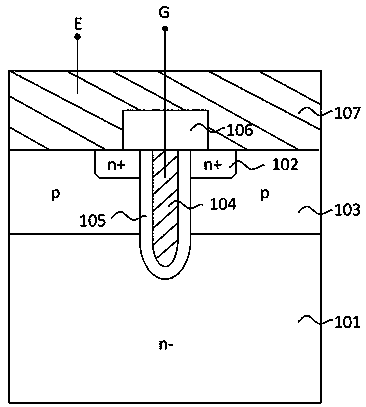
[0054] Figure 1 to Figure 7 An embodiment of the present invention is shown. Such as figure 1 As shown, the semiconductor device is an IGBT, and the semiconductor substrate includes a front structure of the device IGBT and an n-type drift region 101 . The formed front structure includes n-type emitter region 102 , p-type base region 103 , trench gate 104 , gate oxide 105 , insulating layer 106 and front metal electrode 107 . The manufacturing method of the back collector area is the technical feature of the present invention. Specific steps are as follows:

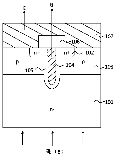
[0055] Step 1. If figure 2 As shown, the ion implantation of the first p-type collector region on the back is carried out, and boron (B) implantation is used. The implantation energy of boron ions is 10KeV-400KeV, for example, it is set as 20KeV-50KeV. The implantation dose of boron ions is 1E13cm -2 ~5E15 cm -2 , for example set to 1E13cm -2 ~2E15 cm -2 .

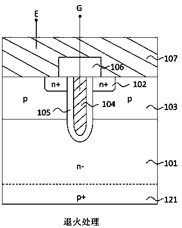
[0056] Step 2. If image 3 As shown, the semiconduc...


PUM


Abstract

The invention relates to the field of semiconductor device manufacturing and particularly relates to a power semiconductor device and a manufacturing method of collector regions thereof. The semiconductor device includes a semiconductor substrate or a semiconductor substrate having an n-type buffer layer formed on a back surface of the semiconductor substrate, a first p-type collector region and asecond p-type collector region. The first p-type collector region is formed by injecting boron into the back surface of the semiconductor substrate, and the second p-type collector region is formed by injecting aluminum into the back surface of the semiconductor substrate. From the back surface of the semiconductor substrate, the peak position of the aluminum injection is shallower than the peakposition of the boron injection. The peak concentration of the aluminum injection is higher than the peak concentration of the boron injection. The first p-type collector region is formed through boron injection, and the second p-type collector region is formed through aluminum injection. The carrier concentration of the collector regions can be effectively increased under the condition that the annealing temperature range is not exceeded. As a result, the hole injection efficiency of an IGBT device and the conductivity modulation effect of a drift region are improved. The lower conduction voltage drop and the lower on-state loss are realized.

Description

technical field [0001] The invention relates to the field of semiconductor device manufacturing, in particular to a method for manufacturing a power semiconductor device and a collector region thereof. Background technique [0002] For bipolar semiconductor devices, such as diodes or insulated gate bipolar transistors (IGBT, insulated gate bipolar transistor), the injection of minority carrier holes from the collector region to the drift region is realized through the formation of the p-type collector region on the back, combined with Electron injection into the n-type emitter region on the front of the device can form electron-hole plasma in the drift region, thereby producing a conductance modulation effect, which can greatly reduce the on-resistance of the device, thereby reducing the loss of the device in the on-state state. [0003] In the manufacturing process of semiconductor devices, boron implantation is usually used to form a p-type collector region on the backside...

Claims


Application Information

Patent Timeline
Patent Type & Authority Applications(China)
IPC IPC(8): H01L29/739H01L29/08H01L21/331H01L21/265
CPCH01L21/26513H01L29/0821H01L29/66348H01L29/7397
Inventor 王思亮胡强蒋兴莉
Owner 成都森未科技有限公司
Why Eureka
Try Eureka