High-precision anti-symmetric bimorph structure shape memory alloy and a preparation method thereof

A memory alloy and bimorph technology, which is applied in the field of shape memory alloys with a high-precision antisymmetric bimorph structure and its preparation, can solve the problems of inability to manufacture a high-precision three-dimensional structure, undercutting phenomenon, poor dimensional accuracy, etc. The effect of mass production, lower production costs, and avoidance of external force interference

Active Publication Date: 2019-05-14
NORTHWESTERN POLYTECHNICAL UNIV
View PDF5 Cites 2 Cited by
  • Summary
  • Abstract
  • Description
  • Claims
  • Application Information

AI Technical Summary

Problems solved by technology

However, the currently studied shape memory alloy thin films are basically manufactured by radio frequency (RF) or direct current (DC) magnetic ion sputtering, and the micro shape memory alloy structures obtained based on this manufacturing method are basically diluted The mixed solution of hydrofluoric acid, nitric acid and deionized water is obtained by corrosion, literature: Fu, Yongqing, Du, Hejun and Hu Min. "TiNi-based thin films in MEMS applications: a review." Sensors and Actuators Vol.112(2004 ):pp.395–408., but this etching method not only has poor dimensional accuracy of the structural features, but also has serious undercutting, and the etching time is too long. At the same time, it is impossible to manufacture high-precision complex three-dimensional structures.

Method used


Image

  • High-precision anti-symmetric bimorph structure shape memory alloy and a preparation method thereof
  • High-precision anti-symmetric bimorph structure shape memory alloy and a preparation method thereof
  • High-precision anti-symmetric bimorph structure shape memory alloy and a preparation method thereof

Examples


Embodiment Construction

[0040] Now in conjunction with embodiment, accompanying drawing, the present invention will be further described:

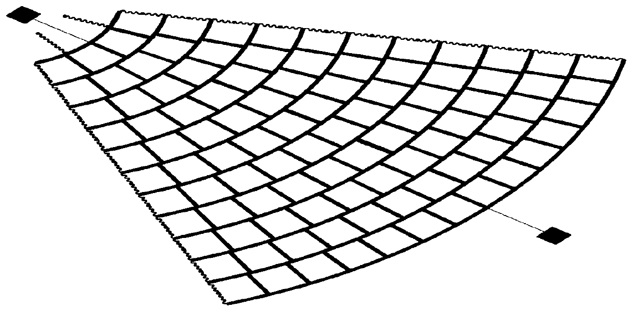
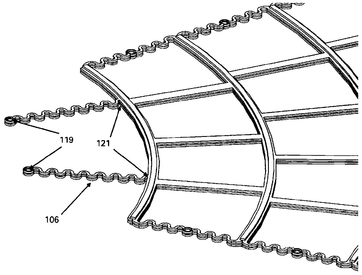
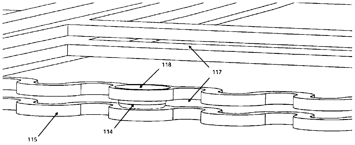
[0041] The specific structure of the embodiment is an anti-symmetric bimorph (Bimorph) structure, including a bottom bimorph shape memory alloy film, a top bimorph shape memory alloy film, and a driving electrode, wherein the driving electrode and the bottom bimorph shape memory alloy film pass through The support beams are fixedly connected, the driving electrodes are fixed on the silicon wafer, the bottom and top double-chip shape memory alloy film structures are antisymmetric, and the two parts are fixedly connected up and down through the anchor point (Anchor), except for the anchor point, the upper and lower double-chip shape The memory alloy thin film does not have any contact points and has gaps, and the shape memory alloy thin film at the bottom is not in contact with the silicon chip and has gaps. The antisymmetric bimorph (Bimorph) structure shape memor...


PUM


Abstract

The invention relates to a high-precision anti-symmetric bimorph structure shape memory alloy and a preparation method thereof. A shape memory alloy film structure is manufactured by using a method ofelectron beam evaporation (E-beam Evaporation) and photoresist stripping (Lift-off Rest). A traditional ion sputtering method is not adopted to deposit the shape memory alloy thin film and then the structure is obtained through wet etching. Therefore, the structural feature size precision obtained by the preparation method provided by the invention only depends on the precision of the photoresist, and as the wavelength of the UV light of the exposure photoresist adopted by the invention is about 500 nanometers, the overall structural size precision reaches 0.5 micrometer and is 100 times of the precision (50 micrometers) of the current manufacturing method.

Description

technical field [0001] The invention belongs to the field of micro-electromechanical system (MEMS) processing and the field of shape-memory alloy smart materials, and relates to a shape-memory alloy with a high-precision antisymmetric double-crystal structure and a preparation method. Background technique [0002] In recent decades, microactuators have been widely used in various fields, such as aerospace, due to their ability to precisely coordinate in a limited microenvironment and finely handle various miniature targets, literature: Kudva, Jayanth N. "Overview of the DARPA Smart Wing Project.” Journal of Intelligent Material Systems and Structures Vol.15No.4(2004):pp.261–267., Biomedical Sciences, Literature: Lorenza, Petrini and Francesco, Migliavacca. “Biomedical Applications of Shape Memory Alloys.” Journal of Metallurgy Vol.1(2011):pp.1–15. and robotics and other fields, literature: Sung-Hyuk, Songand Jang-Yeob, Lee. "35Hz SMA actuator with bending-twisting mode." Sci...

Claims


Application Information

Patent Timeline
Patent Type & Authority Applications(China)
IPC IPC(8): B81B3/00B81C1/00
Inventor 罗建军孙浩师用
Owner NORTHWESTERN POLYTECHNICAL UNIV
Why Eureka
Try Eureka