
Method for improving yield of semiconductor device

A semiconductor and device technology, applied in the field of improving the yield rate of semiconductor devices, can solve problems such as the decline in the yield rate of semiconductor devices

Active Publication Date: 2019-05-17
SHANGHAI HUAHONG GRACE SEMICON MFG CORP
View PDF8 Cites 2 Cited by
  • Summary
  • Abstract
  • Description
  • Claims
  • Application Information

AI Technical Summary

Problems solved by technology

[0005] The purpose of the present invention is to provide a method for improving the yield rate of semiconductor devices, to solve the semiconductor problem caused by the height of the shallow trench isolation in the prior art being too high or too low when adjusting the height of the shallow trench isolation in the flash memory. The problem of device yield decline

Method used


Image

  • Method for improving yield of semiconductor device
  • Method for improving yield of semiconductor device
  • Method for improving yield of semiconductor device

Examples


Embodiment Construction

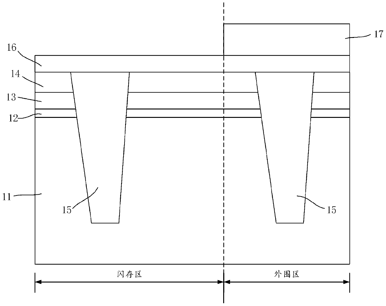
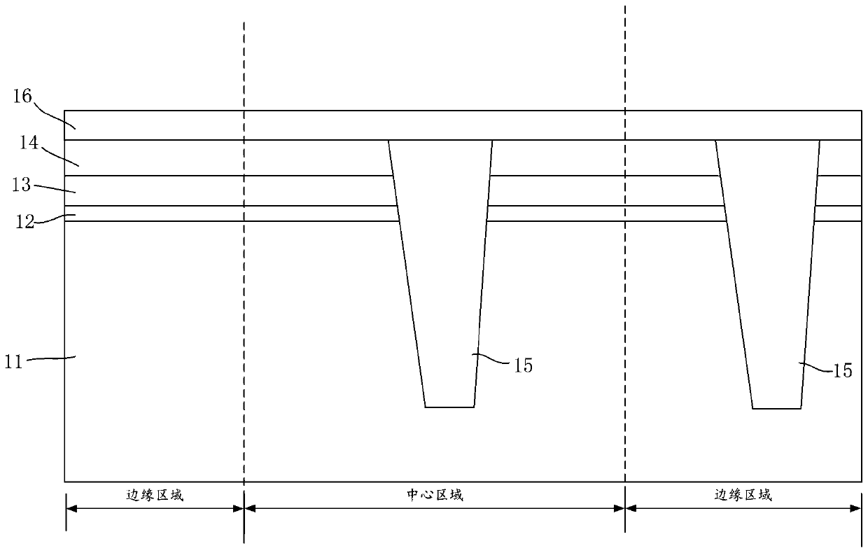
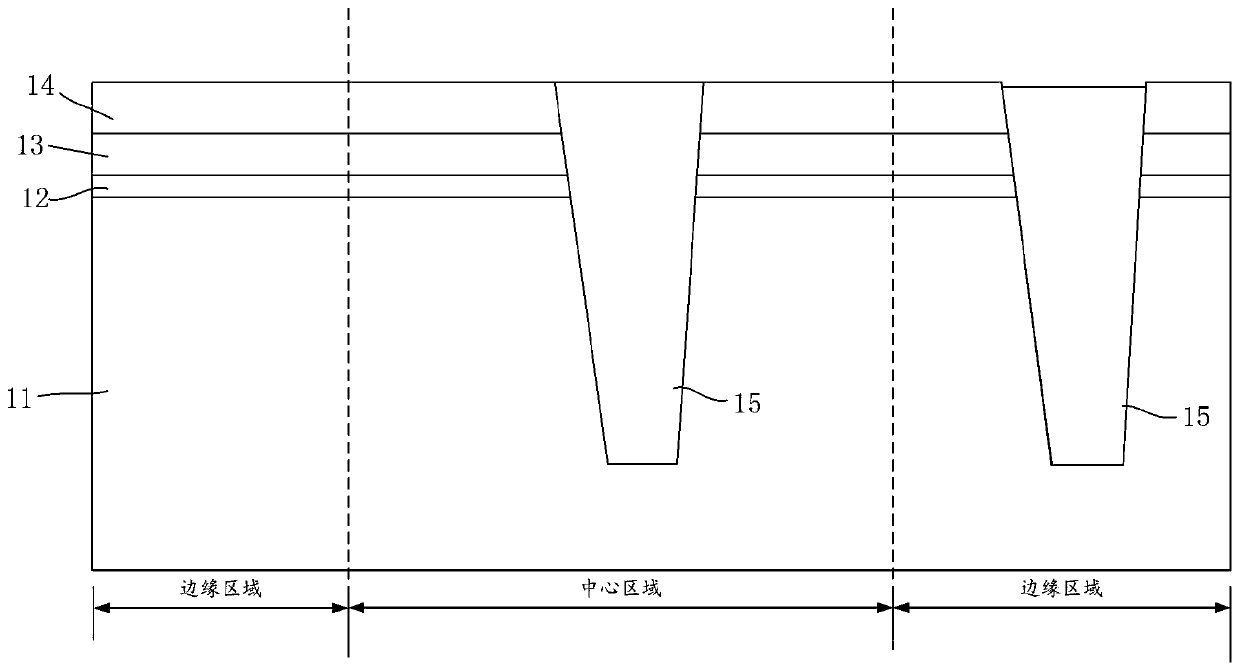
[0031] The specific implementation manner of the present invention will be described in more detail below with reference to schematic diagrams. The advantages and features of the present invention will be more apparent from the following description. It should be noted that all the drawings are in a very simplified form and use imprecise scales, and are only used to facilitate and clearly assist the purpose of illustrating the embodiments of the present invention.

[0032] In the following description, it will be understood that when a layer (or film), region, pattern or structure is referred to as being "on" a substrate, layer (or film), region and / or pattern, it can be directly on another layer or substrate, and / or intervening layers may also be present. Further, it will be understood that when a layer is referred to as being 'under' another layer, it can be directly under, and / or one or more intervening layers may also be present. In addition, designations regarding 'on' ...


PUM


Abstract

The invention provides a method for improving the yield of a semiconductor device, which comprises the following steps: providing a substrate, and sequentially forming a dielectric layer, a floating gate layer and an interlayer dielectric layer on the substrate; forming a mask layer on the surface of the interlayer dielectric layer and the surface of a shallow trench isolation, wherein the substrate comprises a central area and an edge area, and the thickness of the mask layer in the edge area is larger than that of the mask layer in the center of the substrate and the central area; and sequentially etching the mask layer and part of the shallow trench isolation until the shallow trench isolation reaches a standard height. The method for improving the yield of the semiconductor device finally enables the height of the residual shallow trench isolation in the edge area of the substrate and the height of the residual shallow trench isolation in the central area of the substrate to reachthe standard, avoids the failure of the semiconductor device and improves the yield of the semiconductor device.

Description

technical field [0001] The invention relates to the field of semiconductor manufacturing, in particular to a method for improving the yield of semiconductor devices. Background technique [0002] In the current semiconductor industry, memory devices account for a considerable proportion of integrated circuit products. The development of flash memory in memory is particularly rapid. Its memory cell is based on the traditional MOS transistor structure, adding a floating gate (Floating Gate, FG) and a layer of tunnel oxide layer (Tunnel Oxide), and using the floating gate to store charges to achieve non-volatile storage. However, a Shallow Trench Isolation (STI, Shallow Trench Isolation) structure is required between memory cells for electrical isolation. [0003] The flash memory is divided into two types: a stackgate device and a splitgate device. The stackgate device has a floating gate and a control gate, and the control gate is located above the floating gate. In the sp...

Claims


Application Information

Patent Timeline
IPC IPC(8): H01L21/762H01L27/11531
Inventor 陈宏
Owner SHANGHAI HUAHONG GRACE SEMICON MFG CORP
Learn More