A method for precise fabrication of nanopores
A manufacturing method and nanopore technology, which are applied in the fields of nanostructure manufacturing, nanotechnology, nanotechnology, etc., can solve the problems of inability to precisely locate, difficult to accurately control the electron beam nanopore, and uncertainty of use parameters, and achieve application Wide range, precise manufacturing, simple and efficient manufacturing methods
- Summary
- Abstract
- Description
- Claims
- Application Information
AI Technical Summary
Problems solved by technology
Method used
Image
Examples
Embodiment 1
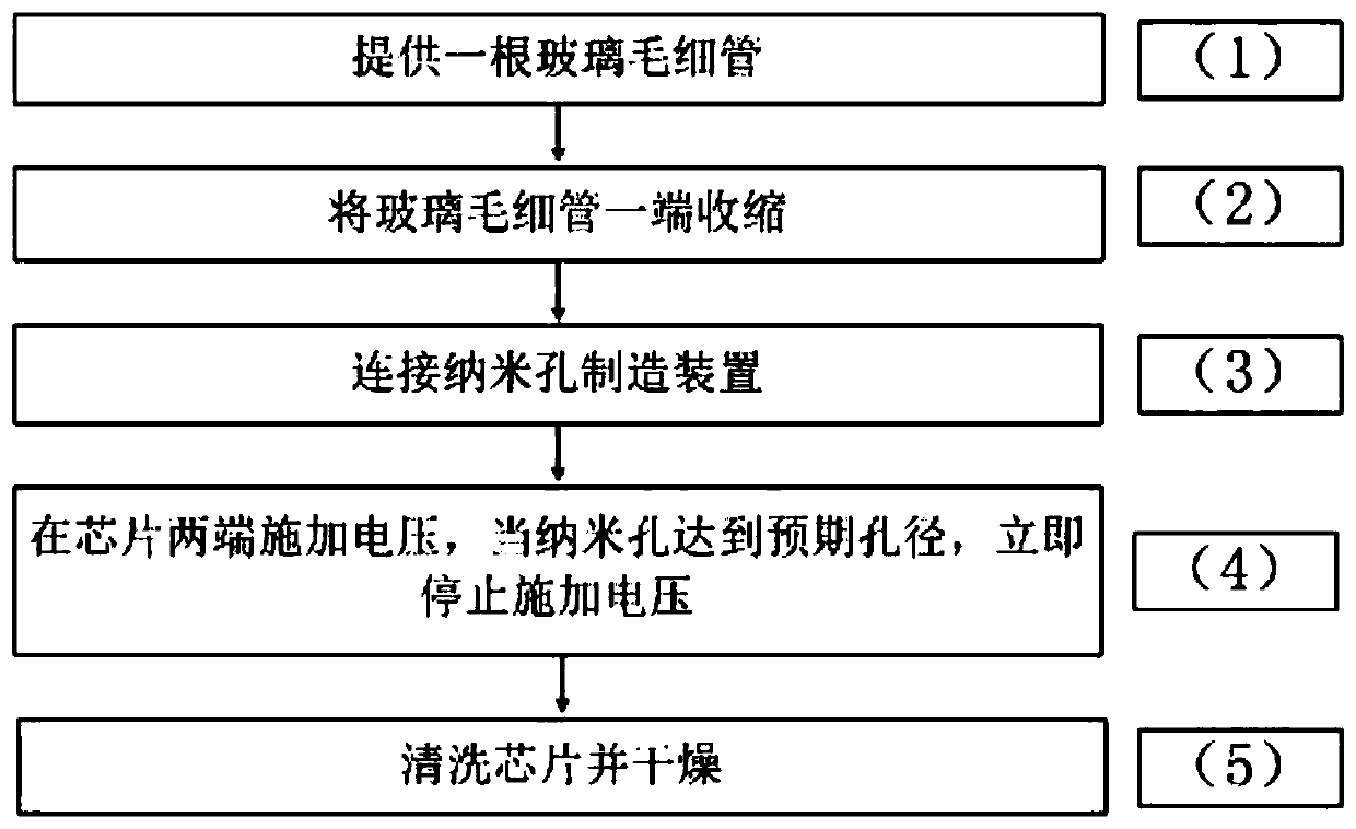
[0042] A method for the precise fabrication of nanopores, such as Figure 1~5 shown, including the following steps:
[0043] (1) Provide a glass capillary;
[0044] (2) Shrink one end of the glass capillary;
[0045] (3) Connect the nanopore manufacturing device;
[0046] (4) Apply voltage at both ends of the chip, and stop applying voltage immediately when the nanopore reaches the expected pore size;
[0047] (5) Clean the chip and dry it;
[0048] The nanopore structure of this embodiment and its manufacturing method will be described in detail below in conjunction with specific drawings.
[0049] First perform step (1), providing a glass capillary 1, such as figure 2 shown. The cross-sectional shape of the glass capillary 1 is circular; the cross-sectional diameter of the glass capillary 1 is 500 nm.
[0050] Then perform step (2), shrink one end of the glass capillary 1, such as image 3shown. The contraction method is: electron beam contraction, the electron bea...
Embodiment 2
[0055] This embodiment is the second embodiment of the nanopore precise manufacturing method of the present invention. The difference from Embodiment 1 is that the voltage of the electron beam is 0.5 kV, the current of the electron beam is 0.5 µA, the continuous scanning time is 500 s, and the scanning area 20 µm×20 µm, the vertical distance from the objective lens to the highest point of the sample is 2 mm, the scanning speed is 0.01 s, and the diameter of one end of the glass capillary 1 after contraction is 500 nm; the applied voltage is: 0.1 V;
[0056] Other steps and operations are the same as in Example 1.
Embodiment 3
[0058] This embodiment is the second embodiment of the nanopore precise manufacturing method of the present invention. The difference from Embodiment 1 is that the voltage of the electron beam is 20 kV, the current of the electron beam is 50 µA, the continuous scanning time is 5 s, and the scanning area is 10 µm×10 µm, the vertical distance from the objective lens to the highest point of the sample is 15 mm, the scanning speed is 30 s, and the diameter of one end of the glass capillary 1 after contraction is 50 nm; the applied voltage is: 30 V;
[0059] Other steps and operations are the same as in Example 1.
PUM
| Property | Measurement | Unit |
|---|---|---|
| thickness | aaaaa | aaaaa |
| diameter | aaaaa | aaaaa |
| diameter | aaaaa | aaaaa |
Abstract
Description
Claims
Application Information


