White LED chip structure and manufacturing method thereof

An LED chip and manufacturing method technology, applied to semiconductor devices, electrical components, circuits, etc., can solve the problems of image color distortion, cumbersome process, phosphor aging, etc., to avoid energy loss, simple manufacturing process, and high luminous efficiency. Effect

Active Publication Date: 2019-06-04
BYD SEMICON CO LTD
View PDF3 Cites 0 Cited by
  • Summary
  • Abstract
  • Description
  • Claims
  • Application Information

AI Technical Summary

Problems solved by technology

[0004] The above-mentioned technology of using blue LED+yellow phosphor to obtain white light, on the one hand, lacks red light as one of the three primary colors of white light, so it is usually called false white light, and the color of the irradiated image will be distorted. On the other hand, the above-mentioned method of obtaining white light The technology uses blue light to excite yellow phosphors, and there will be energy loss in the process of using high-energy blue light to excite yellow phosphors to obtain low-energy yellow light, so the luminous efficiency will not be too high, and the lost energy conversion In order to generate heat, the luminous efficiency of the LED is seriously affected, and the aging phenomenon of the phosphor powder is serious. Therefore, more methods are usually required to reduce the effect of heat generation on the performance of the LED during the device manufacturing process, which is affected by the aging life of the phosphor powder. , the life of ordinary white LED is only 30,000 to 50,000 hours, while the life of general chip can reach 80,000 to 100,000 hours, so the application of phosphor seriously affects the life of LED
And due to the use of phosphor powder, there are more packaging processes such as phosphor powder coating, crystal bonding, and wire bonding, the process is more cumbersome and the cost is higher

Method used


Image

  • White LED chip structure and manufacturing method thereof
  • White LED chip structure and manufacturing method thereof
  • White LED chip structure and manufacturing method thereof

Examples


Embodiment Construction

[0021] Embodiments of the invention are described in detail below, examples of which are illustrated in the accompanying drawings. The embodiments described below by referring to the figures are exemplary and are intended to explain the present invention and should not be construed as limiting the present invention.

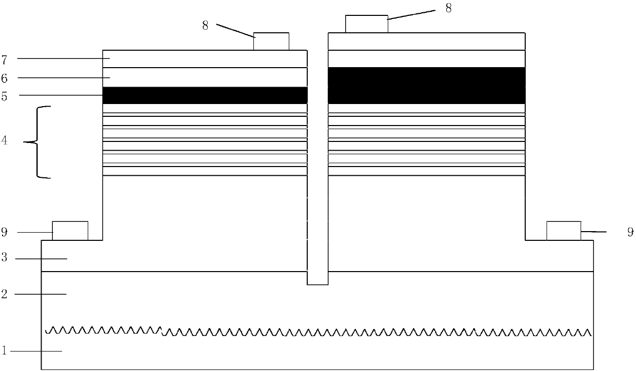
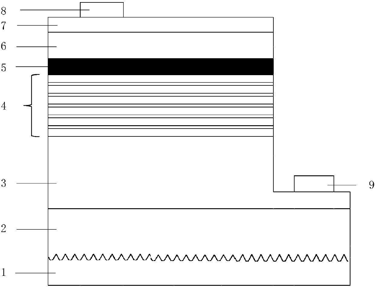
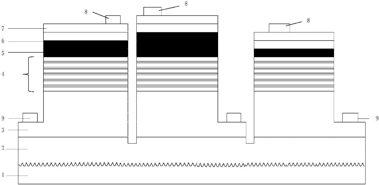
[0022] Such as figure 2 As shown, Embodiment 1 of the present invention provides a white light LED chip structure. At least two sub-chips are provided on the same LED chip. The sub-chips include a substrate 1 and an epitaxial layer formed on the substrate. The epitaxial layer is provided with The electron blocking layer 5 and the light-emitting layer 4, by setting the thickness of the electron blocking layer 5 of different sub-chips, cooperate with the light-emitting layer 4, different sub-chips can emit light of different wavelengths, and the lights of different wavelengths are mixed to form white light.

[0023] A white light LED chip structure provided by Em...


PUM


Abstract

The invention provides a white LED chip structure and a manufacturing method thereof. At least two sub-chips are disposed on the same LED chip, each of the sub-chips comprises a substrate and an epitaxial layer formed on the substrate, an electron blocking layer and a light-emitting layer are disposed in the epitaxial layer, different sub-chips can emit light of different wavelengths with the cooperation with the light-emitting layer by setting the thickness of the electron blocking layers of different sub-chips. Compared with a traditional LED chip structure, the white light can be achieved by using a single chip, a condition that a traditional LED chip needs phosphor to realize white light is avoided, therefore, the problems of aging, falling and the like caused by the phosphor are avoided, the process is simple, the energy loss during the excitation process of the phosphor is avoided, and the luminous efficiency is higher. Compared with a mode of achieving white light by a traditional three-primary-color chip, the invention has the advantages that the white light can be achieved by using the single chip, and the manufacturing process is simpler.

Description

technical field [0001] The invention belongs to the technical field of LED chips, and in particular relates to a structure and a manufacturing method of a white light LED chip. Background technique [0002] Light-emitting diode (LED) is a junction-type electroluminescent semiconductor device that can convert electrical signals into optical signals. Gallium nitride (GaN)-based light-emitting diodes, as solid-state light sources, have been recognized for their high efficiency, long life, energy saving and environmental protection. , small size and other advantages are known as another revolution in the history of human lighting after Edison invented the electric light, and have become the focus of research and development and industry in the international semiconductor and lighting fields. Gallium nitride (GaN), indium gallium nitride (InGaN) , aluminum gallium nitride (AlGaN) and aluminum indium gallium nitride (AlGaInN)-based III-V nitride materials have a continuously adjus...

Claims


Application Information

Patent Timeline
Patent Type & Authority Applications(China)
IPC IPC(8): H01L27/15H01L33/14H01L33/00
Inventor 谢春林
Owner BYD SEMICON CO LTD
Why Eureka
Try Eureka