
Method for casting polycrystalline silicon ingot based on quasi-single crystal semi-melting technology

A polycrystalline silicon ingot, quasi-single crystal technology, applied in the growth of polycrystalline materials, chemical instruments and methods, crystal growth, etc., can solve the problems of less single feeding, short life, complicated operation, etc. Effect

Inactive Publication Date: 2019-06-07
江苏金晖光伏有限公司
View PDF0 Cites 0 Cited by
  • Summary
  • Abstract
  • Description
  • Claims
  • Application Information

AI Technical Summary

Problems solved by technology

Polysilicon ingot casting has large feeding capacity, simple operation, and low process cost, but the battery conversion efficiency is low and the service life is short; Czochralski monocrystalline silicon conversion efficiency is high, but single feeding is small, the operation is complicated, and the cost is high

Method used


Image

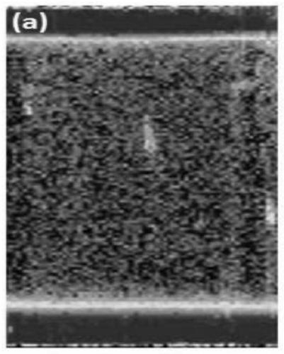
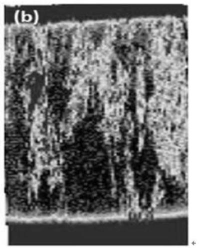
  • Method for casting polycrystalline silicon ingot based on quasi-single crystal semi-melting technology
  • Method for casting polycrystalline silicon ingot based on quasi-single crystal semi-melting technology
  • Method for casting polycrystalline silicon ingot based on quasi-single crystal semi-melting technology

Examples


Embodiment Construction

[0041] The method for casting polycrystalline silicon ingots based on quasi-single crystal semi-melting technology of the present invention uses the principle of single crystal production to carry out polycrystalline ingot casting, and takes the millimeter-scale seed crystal as the nucleation center to perform outer edge growth seeding, on the same cross section Alleviate the dislocation proliferation, subgrain boundary and self-interstitial atoms caused by the large thermal stress at the edge of the silicon ingot, reduce the length of the red area at the bottom, and improve the electrical conductivity of polysilicon.

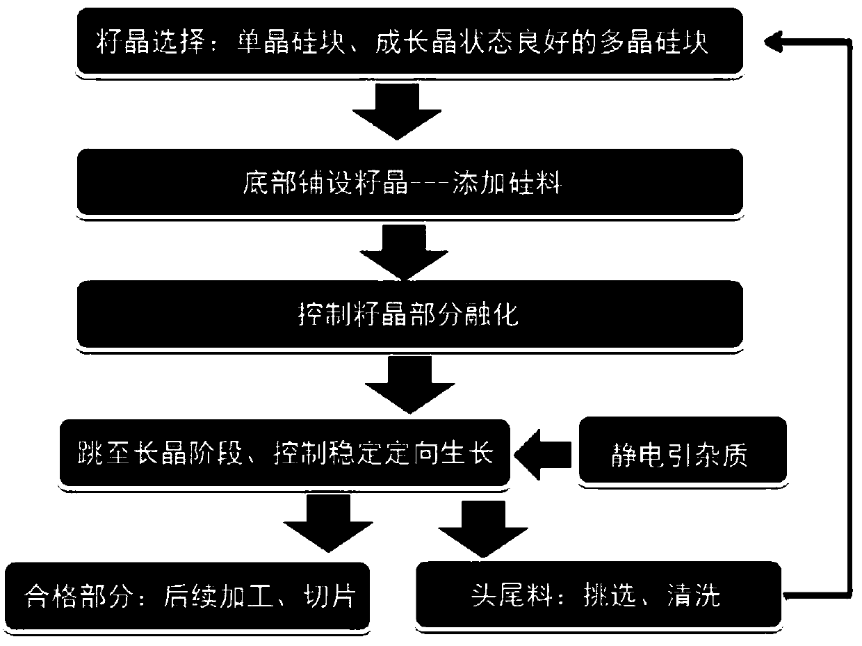
[0042] Such as figure 2 Shown, the method for casting polycrystalline silicon ingot based on quasi-single crystal semi-melting technology of the present invention, it comprises the following technical contents:

[0043] Step 1 Seed selection

[0044] Choose monocrystalline silicon blocks and polycrystalline silicon blocks with good growth conditions.

[0045...


PUM


Abstract

The invention provides a method for casting a polycrystalline silicon ingot based on the quasi-single crystal semi-melting technology. the method comprises the following steps: step 1, seed crystal selection: selecting a single crystal silicon block and a polycrystalline silicon block with a good growth state; step 2, laying seed crystals at the bottom of ingot casting equipment and adding a silicon material; step 3, controlling partial melting of the seed crystals; step 4, jumping to a crystal growth stage and controlling the steady directional growth; and step 5, selecting qualified polycrystalline silicon ingot products for subsequent processing and slicing. According to the method, the single crystal production principle is utilized to produce the polycrystalline ingot, the millimeterseed crystals are used as nucleation centers for edge growth crystal induction, the dislocation multiplication, sub-grain boundary and self-interstitial atoms caused by the relatively large thermal stress at the edge of the silicon ingot are alleviated on the same cross section, the length of the bottom red zone is reduced, and the conductivity of the polycrystalline silicon is improved.

Description

technical field [0001] The invention belongs to the technical field of photovoltaic polysilicon manufacturing, and in particular relates to a method for casting polysilicon ingots based on quasi-single crystal semi-melting technology. Background technique [0002] Today, with the rapid development of the photovoltaic industry, the crystalline silicon used to manufacture solar cells is mainly monocrystalline silicon using the Czochralski method and polycrystalline silicon using ingot technology. Polysilicon ingot casting has large feeding capacity, simple operation, and low process cost, but the battery conversion efficiency is low and the service life is short; Czochralski monocrystalline silicon conversion efficiency is high, but single feeding is small, the operation is complicated, and the cost is high. Therefore, how to combine the two into one has become a hot and difficult point for domestic and foreign photovoltaic companies to study. In this case, quasi-single crysta...

Claims


Application Information

Patent Timeline
IPC IPC(8): C30B28/06C30B29/06
Inventor 刘爱军曹丙强庄艳歆周浪
Owner 江苏金晖光伏有限公司
Learn More