AlGaInP red light-emitting diode device structure with composite reflector

A compound mirror and red light-emitting technology, which is applied in the direction of semiconductor devices, electrical components, circuits, etc., can solve the problems of sacrificing the reflectivity of the mirror layer, the light output efficiency of the device, and insufficient adhesion

Active Publication Date: 2019-06-11
NANCHANG UNIV +1
View PDF5 Cites 0 Cited by
  • Summary
  • Abstract
  • Description
  • Claims
  • Application Information

AI Technical Summary

Problems solved by technology

However, Ag or Ag-based materials with higher reflectivity have not been adopted due to insufficient adhesion to the dielectric reflective layer, thus sacrificing the reflectivity of the mirror layer and the light extraction efficiency of the device.

Method used


Image

  • AlGaInP red light-emitting diode device structure with composite reflector
  • AlGaInP red light-emitting diode device structure with composite reflector
  • AlGaInP red light-emitting diode device structure with composite reflector

Examples


Embodiment 1

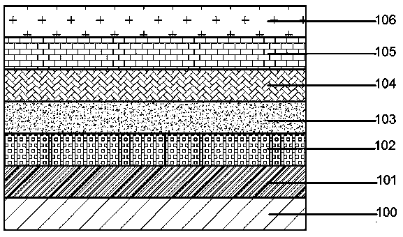
[0040] 1. Epitaxial growth: First, on the GaAs substrate 100, a GaInP etch stop layer 101, a GaAs ohmic contact layer 102, an n-type AlGaInP main layer 103, an active layer 104, a p-type AlGaInP main layer 105, and a p-type GaP ohmic contact are sequentially grown on the GaAs substrate 100. Layer 106, such as figure 1 shown;

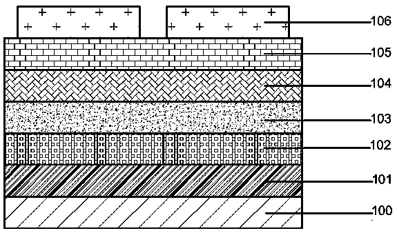
[0041]2. Current blocking photolithography: etching the p-type GaP ohmic contact layer 106 in the area directly under the edge and the designed n-electrode 113 to expose the p-type AlGaInP main layer 105, such as figure 2 As shown, the remaining thickness of the p-type semiconductor layer is 0.5 μm-2.5 μm, and the doping concentration of the p-type AlGaInP main layer 105 exposed after etching is less than 1×10 19 / cm 3 ;

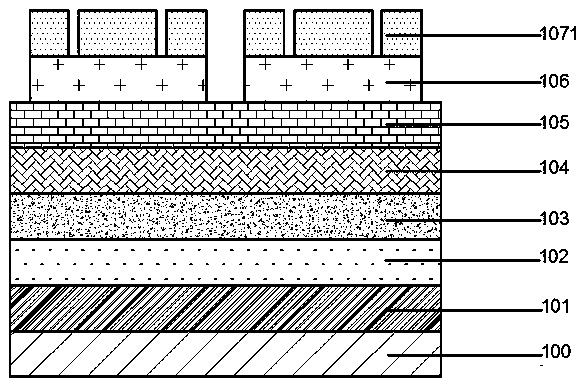
[0042] 3. Preparation of dielectric layer 1071: grow a layer of SiO by plasma-assisted chemical vapor deposition (PECVD) 2 The dielectric layer 1071 as the composite mirror layer has a thickness of 50-500 nm; in the reserved area ...

Embodiment 2

[0048] 1. Epitaxial growth: First, on the GaAs substrate 100, a GaInP etch stop layer 101, a GaAs ohmic contact layer 102, an n-type AlGaInP main layer 103, an active layer 104, a p-type AlGaInP main layer 105, and a p-type GaP ohmic contact are sequentially grown on the GaAs substrate 100. Layer 106, such as figure 1 shown.

[0049] 2. Current blocking lithography: etching the p-type GaP ohmic contact layer 106 at the edge and the area directly under the designed n-electrode 113 to expose the p-type AlGaInP main layer 105. After etching, the remaining thickness of the p-type semiconductor layer is 0.5μm-2.5μm, such as figure 2 shown;

[0050] 3. Preparation of the dielectric layer 1071: a layer of SiO is grown on the p-type GaP ohmic contact layer 106 by PECVD 2 The dielectric layer 1071 as a composite mirror layer has a thickness of 90 nm-120 nm; in the reserved area of ​​the p-type GaP ohmic contact layer 106, SiO 2 A round hole is photoetched to expose the p-type GaP ...

Embodiment 3

[0057] 1. Epitaxial growth: First, on the GaAs substrate 100, a GaInP etch stop layer 101, an n-type GaAs ohmic contact layer 102, an n-type AlGaInP main layer 103, an active layer 104, a p-type AlGaInP main layer 105, and a p-type GaP are sequentially grown on the GaAs substrate 100 ohmic contact layer 106, such as figure 1 shown;

[0058] 2. The first transfer: the wafer is transferred to the temporary substrate 116 with wax or other easily removable materials 115; the temporary substrate 116 is sapphire or silicon or other materials that can provide support, such as Figure 11 shown;

[0059] 3. Remove the substrate and cut-off layer: use NH 3 .H 2 O:H 2 o 2 =1:3 or other concentrations that can corrode the GaAs substrate 100, remove the GaAs substrate 100, the temperature is 20-30°C, and the time is 20 min-60 min; use HCl:H3PO4=2:1, remove the GaInP etch stop layer 101 , the temperature is 20-30°C, the time is 1 min-5 min, such as Figure 12 shown;

[0060] 4. Alig...


PUM

PropertyMeasurementUnit
thicknessaaaaaaaaaa
thicknessaaaaaaaaaa
thicknessaaaaaaaaaa

Abstract

The invention discloses an AlGaInP red light-emitting diode device structure with a composite reflector. The reflector of a conventional AlGaInP red light-emitting diode is changed into a composite reflector layer, the composite reflector layer is divided into a reflection area, an electrode and an adhesion area, the reflection area consists of a dielectric layer and a reflection metal, the refractive index of the dielectric material of the dielectric layer is between 1.0 and 2.5, the electrode is metal, the material is related to a contacted semiconductor material, for p-type GaP, the metal material of the electrode is Au or AuZn alloy or stacking layer of Au and AuZn alloy, or, the metal material of the electrode is Ag or NiAg stacking layer or TiAg stacking layer; for n-type GaAs, the metal material of the electrode is a stacking layer of three metals such as Ni, Au and Ge or alloy of two or more than two of Ni, Au and Ge; and the adhesion material of the adhesion area is one of Cr,Ti, Ni, Mg, Fe and TiW. The AlGaInP red light-emitting diode device structure has the advantages that the reflection rate of the reflector and the light outgoing efficiency and electro-optical conversion efficiency of the device are improved and simultaneously the reflector structure has preferable adhesion and reliability.

Description

technical field [0001] The invention relates to a light-emitting diode, in particular to an AlGaInP red light-emitting diode device structure with a compound reflector. Background technique [0002] The AlGaInP-based material lattice-matched with the GaAs substrate is a direct bandgap semiconductor. By adjusting the ratio of Al and Ga, the forbidden band width can be varied between 1.9eV and 2.3eV. The wavelength range of AlGaInP-based LEDs can cover 550nm to 650nm, and has broad application prospects in the fields of RGB three-color display screens, traffic lights, and automotive lights. [0003] The growth of AlGaInP red light-emitting diodes is based on GaAs substrate, and the cut-off layer, n-type GaAs ohmic contact layer, n-type AlGaInP main layer, active layer, p-type GaP main layer and p-type GaP are sequentially grown on the GaAs substrate. Ohmic contact layer. [0004] The GaAs substrate has an absorption effect on red light. In order to improve the light efficien...

Claims


Application Information

Patent Timeline
Patent Type & Authority Applications(China)
IPC IPC(8): H01L33/10H01L33/14
Inventor 吴小明刘军林陈芳江风益
Owner NANCHANG UNIV
Why Eureka
Try Eureka