Deep ultraviolet photodetector for solar blind area based on organic field effect transistor

A technology of deep ultraviolet light and solar blind area, which is used in the manufacture of electric solid state devices, semiconductor devices, semiconductor/solid state devices, etc., to achieve good photoresponsivity and photoselectivity, and enhance photoresponse.

Active Publication Date: 2019-06-14
HEFEI UNIV OF TECH
View PDF7 Cites 2 Cited by
  • Summary
  • Abstract
  • Description
  • Claims
  • Application Information

AI Technical Summary

Problems solved by technology

[0005] The purpose of the present invention is to provide a solar blind zone deep ultraviolet light detector based on organic field effect transistors, to solve the problem that the rigidity of deep ultraviolet light detectors in the prior art limits its application in flexible devices

Method used


Image

  • Deep ultraviolet photodetector for solar blind area based on organic field effect transistor
  • Deep ultraviolet photodetector for solar blind area based on organic field effect transistor
  • Deep ultraviolet photodetector for solar blind area based on organic field effect transistor

Examples


Embodiment Construction

[0032] The present invention will be further described below in conjunction with the accompanying drawings and embodiments.

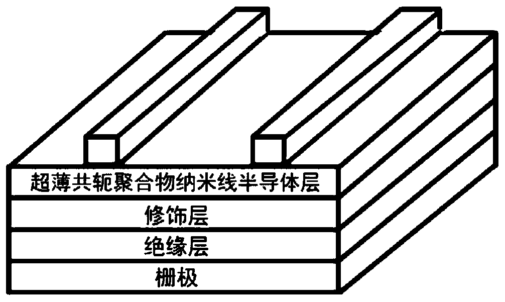
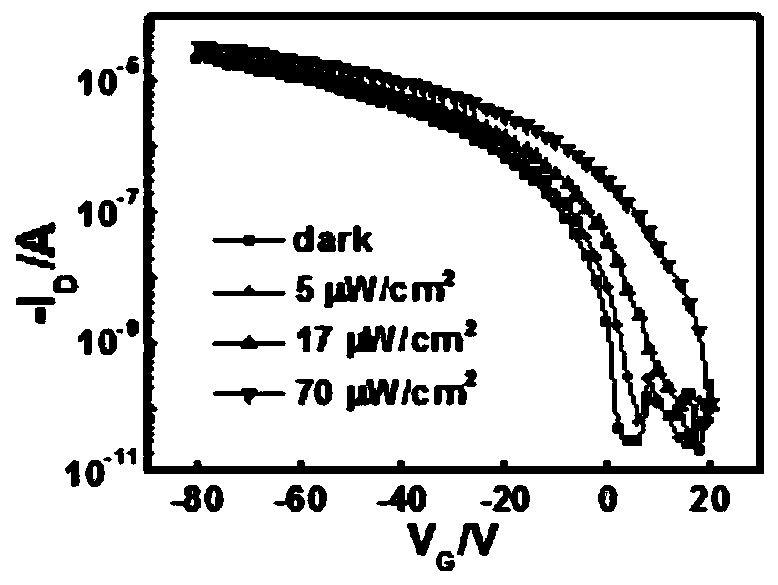
[0033] A solar-blind zone deep ultraviolet photodetector based on an organic field effect transistor, comprising a substrate, a gate electrode, a gate insulating layer, an organic semiconductor layer, a source electrode and a drain electrode, wherein the organic semiconductor layer is prepared on the gate insulating layer Block copolymer semiconductor nanowires, block copolymer semiconductor nanowires are made of block copolymers, the block copolymers are composed of conjugated segments and insulating segments added to the conjugated segment, the insulating segment in the block copolymer It is made of materials that selectively respond to deep ultraviolet light in the solar blind area, and the insulating segment is used as the photosensitive segment.

[0034] In the present invention, the block copolymer is composed of a conjugate segment GED and an ins...


PUM


Abstract

The invention discloses a deep ultraviolet photodetector for a solar blind area based on an organic field effect transistor. An organic field effect transistor semiconductor layer of the deep ultraviolet photodetector is formed by block conjugated polymer nanowires; a block copolymer semiconductor material and a polymer insulating material are respectively dissolved in a solvent and then are mixedto form a blended solution; and block copolymer semiconductor nanowires with different densities are obtained by controlling a mass ratio of the block copolymer semiconductor material to the polymerinsulating material. The block copolymer semiconductor nanowires disclosed by the invention are used as the semiconductor layer of the photodetector based on the organic field effect transistor, so that the optical response to a deep ultraviolet region can be enhanced. According to the deep ultraviolet photodetector, a conjugated polymer is used for responding to deep ultraviolet light of the solar blind area for the first time, and the high-performance deep ultraviolet photodetector for the solar blind area based on the organic field effect transistor is prepared; good light selectivity and light responsiveness are achieved in the deep ultraviolet region, the light response reaches 120 A / W, and the external quantum efficiency is up to 50000%.

Description

technical field [0001] The invention relates to the field of deep ultraviolet photoelectric detectors in sun-blind areas, in particular to a sun-blind area deep-ultraviolet photodetector based on organic field effect transistors. Background technique [0002] The sun-blind spectral region (200-280nm) is defined by a specific band of light that cannot penetrate the atmosphere and reach the Earth's surface. The sun-blind zone deep ultraviolet photoelectric detector equipment has broad application prospects in military surveillance, target detection and acquisition, missile launch detection, remote control, chemical analysis, flame detection, etc. Deep ultraviolet photodetectors are highly responsive to the deep ultraviolet region and are not interfered by ambient visible light or long-wavelength ultraviolet light, which is crucial for tracking the ozone layer hole in the atmosphere. In addition, deep-UV photodetectors have great potential in biological and medical analysis, b...

Claims


Application Information

Patent Timeline
Patent Type & Authority Applications(China)
IPC IPC(8): H01L51/42H01L51/46H01L51/48
CPCY02E10/549
Inventor 邱龙臻赵雪姚宏兵魏诗语王晓鸿
Owner HEFEI UNIV OF TECH
Why Eureka
Try Eureka