Two-dimensional material heterojunction photoelectric detector with surface plasmon and preparation method thereof

A technology of surface plasmons and photodetectors, applied in the field of optical communications, can solve the problems of low light absorption rate, and achieve the effects of simple preparation, improved light response, and enhanced absorption

Active Publication Date: 2021-09-17
UNIV OF ELECTRONICS SCI & TECH OF CHINA
View PDF11 Cites 2 Cited by
  • Summary
  • Abstract
  • Description
  • Claims
  • Application Information

AI Technical Summary

Problems solved by technology

However, due to the atomic-level thickness and transparent properties, light easily passes through two-dimensional materials without being absorbed, so two-dimensional materials face the problem of low light absorption rate.

Method used


Image

  • Two-dimensional material heterojunction photoelectric detector with surface plasmon and preparation method thereof
  • Two-dimensional material heterojunction photoelectric detector with surface plasmon and preparation method thereof
  • Two-dimensional material heterojunction photoelectric detector with surface plasmon and preparation method thereof

Examples


Embodiment Construction

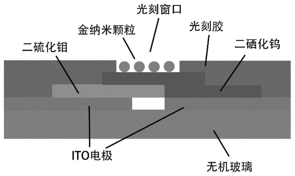
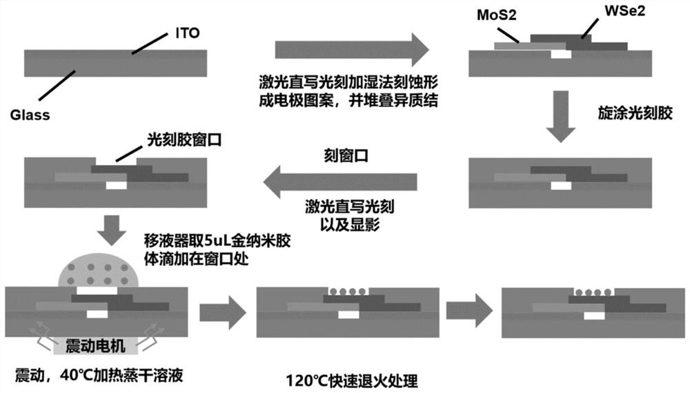
[0015] figure 1 is a structural diagram of a tungsten diselenide / molybdenum disulfide heterojunction photodetector with surface plasmons. The devices are inorganic glass, ITO electrode, molybdenum disulfide, tungsten diselenide, photoresist and gold nanoparticles from bottom to top. exist figure 1 In the structure shown in the figure, the patterned ITO electrode and heterojunction are prepared by depositing an ITO film on the inorganic glass, throwing a layer of positive photoresist, and then using laser direct writing lithography technology to write on the photoresist. The pattern opposite to the electrode pattern is photoetched on the top, and then the ITO covered with the photoresist is put into the etching solution for wet etching, and finally the patterned ITO electrode is obtained by removing the glue. The two-dimensional layered tungsten diselenide and molybdenum disulfide materials were prepared by exfoliating the bulk materials by mechanical exfoliation, and then tr...


PUM


Abstract

The invention relates to a tungsten diselenide / molybdenum disulfide heterojunction photoelectric detector with surface plasmon and a preparation method of the tungsten diselenide / molybdenum disulfide heterojunction photoelectric detector. The tungsten diselenide / molybdenum disulfide heterojunction photoelectric detector comprises an ITO electrode, a heterojunction and gold nanoparticles, wherein the heterojunction is formed by combining two-dimensional tungsten diselenide and molybdenum disulfide through Van der Waals force and by introducing the surface plasmon. According to the photoelectric detector provided by the invention, the light absorption and the light response of the two-dimensional tungsten diselenide / molybdenum disulfide heterojunction are enhanced by utilizing the absorption effect of surface plasmons on photon energy. The preparation method provided by the invention comprises the following steps: accurately etching a window with a submicro-size specific pattern, such as a rectangle or a circle, on photoresist in a heterojunction region through a laser direct writing photoetching technology, and dropwise adding a nano-particle solution, such as a gold nano-particle solution or a silver nano-particle solution, in a window region by using a pipettor; introducing the surface plasmon on the heterojunction region in a manner of enriching the gold nanoparticles in a rectangular window in a vibration and heating environment. The structure of the two-dimensional material heterojunction photoelectric detector with the surface plasmon and the preparation method of the two-dimensional material heterojunction photoelectric detector have the advantages of being novel and simple.

Description

technical field [0001] The invention belongs to the technical field of optical communication, and in particular relates to a photoelectric detector. Background technique [0002] A photodetector is a device that converts optical signals into electrical signals, and it plays a very important role in the fields of optical communication, remote sensing systems, and video imaging. Traditional photodetectors are based on silicon materials, but since silicon is an indirect bandgap semiconductor with a forbidden band width of only about 1.1eV, the detection range of this type of photodetector can only range from visible light to near-infrared light, and the light absorption efficiency low. The two-dimensional semiconductor materials emerging in recent years can overcome the limitation of silicon materials. Such materials usually have atomic-scale thickness and exhibit good optoelectronic properties, so they have received extensive attention in the fabrication of micro-nano optoele...

Claims


Application Information

Patent Timeline
Patent Type & Authority Applications(China)
IPC IPC(8): H01L31/0232H01L31/109H01L31/032H01L31/18
CPCH01L31/02327H01L31/109H01L31/032H01L31/18Y02P70/50
Inventor 黄文肖昊东龚天巡张晓升林媛
Owner UNIV OF ELECTRONICS SCI & TECH OF CHINA
Why Eureka
Try Eureka