

Preparation method of high temperature resistant QFN package structure
A technology of packaging structure and high temperature resistance, which is used in semiconductor/solid-state device manufacturing, electrical components, electrical solid-state devices, etc., can solve problems such as excessive pads and short circuits, reduce usage, improve cross-linking density, and improve mechanical properties. performance effect
- Summary
- Abstract
- Description
- Claims
- Application Information
AI Technical Summary
Problems solved by technology
Method used
Image

Examples
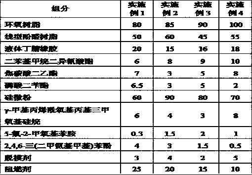
Embodiment 1~4
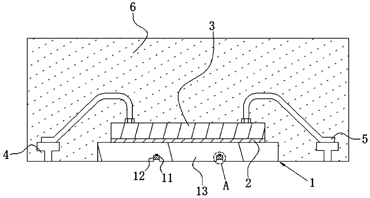
[0028] Embodiments 1 to 4: A preparation method of a high temperature resistant QFN packaging structure, the high temperature resistant QFN packaging structure includes a heat dissipation pad 1, a chip 3 and a conductive pad 4 located in an epoxy insulator 6, and the chip 3 is located in On the heat dissipation pad 1, and the silver paste layer 2 is arranged between the chip 3 and the heat dissipation pad 1, and several conductive pads 4 are arranged on the periphery of the heat dissipation pad 1, and the conductive pad 4 and the chip 3 pass through A lead wire 5 is connected;
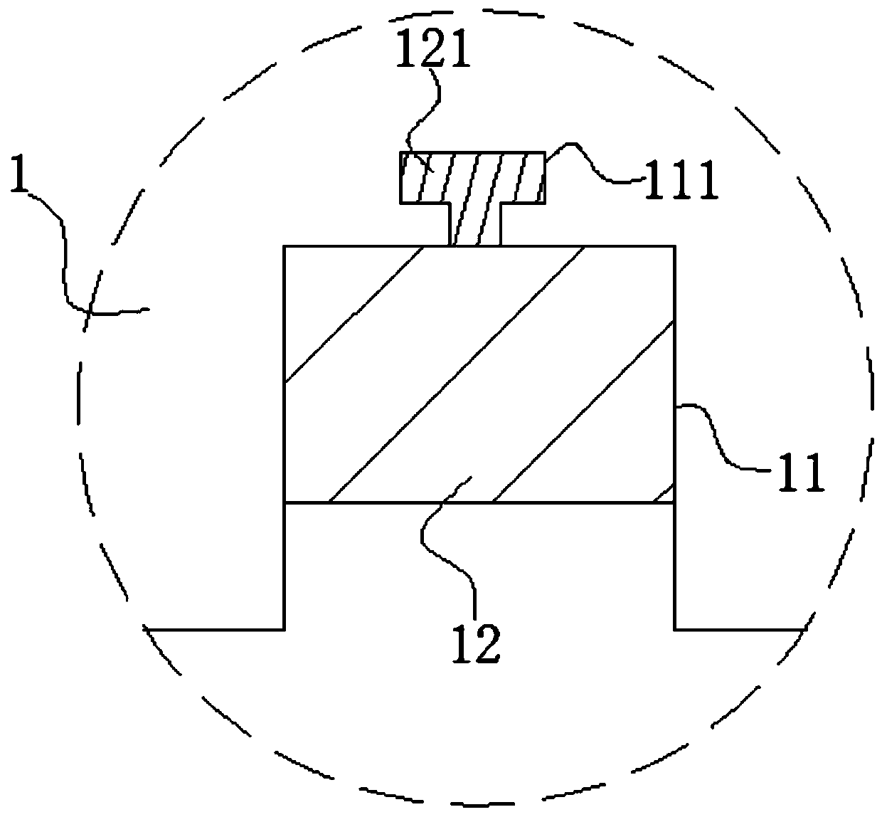
[0029] The side of the heat dissipation pad 1 away from the chip 3 is provided with a separation groove 11, the width of the separation groove 11 is 0.1-0.3 mm, and the separation groove 11 divides the side of the heat dissipation pad 1 away from the chip 3 into equal parts. At least two single pads 13, the separation grooves 11 are filled with heat-conducting insulating strips 12, the walls of the sep...
PUM
| Property | Measurement | Unit |
|---|---|---|
| Area | aaaaa | aaaaa |
Abstract
Description
Claims
Application Information