High-barrier high-thermal-conductivity packaging structure for flexible OLED display and preparation method thereof
A packaging structure and display technology, which is applied in semiconductor/solid-state device manufacturing, identification devices, semiconductor devices, etc., can solve problems such as poor heat dissipation performance, achieve excellent barrier performance, prevent aging, and improve the effect of heat conduction rate
- Summary
- Abstract
- Description
- Claims
- Application Information
AI Technical Summary
Problems solved by technology
Method used
Image


Examples
Embodiment 1
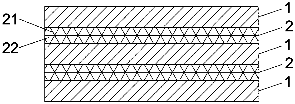
[0040] This embodiment provides a flexible OLED display with high barrier and high thermal conductivity packaging structure, such as figure 1 As shown, it consists of an inorganic passivation layer 1 and a composite buffer layer 2. In order to improve the water and oxygen barrier performance of OLED devices and improve the flatness of the film-forming substrate, it is necessary to alternately stack at least two inorganic passivation layers 1 and at least one composite buffer layer 2, and the ratio of the number of inorganic passivation layers 1 to The composite buffer layer 2 has one more layer, so that the outermost layer of the packaging structure is the inorganic passivation layer 1 . Wherein, the number of layers of the inorganic passivation layer 1 is 5 layers, and the number of layers of the composite buffer layer 2 is 4 layers.
[0041] The luminous efficiency of OLED devices cannot reach 100% during operation, and a large part of the electric energy is converted into ...
Embodiment 2
[0050] This embodiment provides a method for preparing the packaging structure as in Embodiment 1, including:
[0051] (1) Preparation of the first inorganic passivation layer
[0052] Specifically, a flexible substrate containing an OLED display layer is provided, and the first inorganic passivation layer is formed on the flexible substrate and the OLED display layer by chemical vapor deposition, and the film-forming temperature of the first inorganic passivation film layer is 115°C. The thickness of the film is 1 μm, which protects various functional materials of the OLED display layer.
[0053] (2) Prepare the first layer of composite buffer layer
[0054] Specifically, the graphene oxide fiber, the first organic material, the second organic material and the solvent dimethyl sulfoxide are mixed according to a mass ratio of 1:0.3:60:350 and then spin-coated on the first layer of inorganic material in step (1). On the passivation layer, bake at 140° C. for 20 minutes to for...
Embodiment 3
[0063] The present invention provides a high-barrier and high-thermal-conduction packaging structure for flexible OLED displays. Unlike Embodiment 1, the number of layers of the composite buffer layer 2 can also be set to 1 layer, 2 layers, or 3 layers. Correspondingly, the inorganic passivation layer The number of layers of 1 is set to 2 layers, 3 layers, or 4 layers, as long as the number of layers of the inorganic passivation layer 1 is one more than the number of layers of the composite buffer layer 2 so that the outermost layer of the packaging structure is the inorganic passivation layer 1 That's it.
[0064] As a further modification of an alternative embodiment, the thickness of the composite buffer layer 2 can be set to 4 μm, 5 μm, 7 μm, or 8 μm, and the thickness of each composite buffer layer 2 can be the same or different;
[0065] The thickness of the inorganic passivation layer 1 can also be set to 0.5 μm, 0.65 μm, 0.95 μm, etc., and the thickness of each inorgan...
PUM
| Property | Measurement | Unit |
|---|---|---|
| diameter | aaaaa | aaaaa |
| length | aaaaa | aaaaa |
| thickness | aaaaa | aaaaa |
Abstract
Description
Claims
Application Information
 - R&D
- Intellectual Property
- Life Sciences
- Materials
- Tech Scout
- Unparalleled Data Quality
- Higher Quality Content
- 60% Fewer Hallucinations
Browse by: Latest US Patents, China's latest patents, Technical Efficacy Thesaurus, Application Domain, Technology Topic, Popular Technical Reports.
© 2025 PatSnap. All rights reserved.Legal|Privacy policy|Modern Slavery Act Transparency Statement|Sitemap|About US| Contact US: help@patsnap.com