A kind of flexible transparent conductive film with hierarchical structure and preparation method thereof
A kind of technology of transparent conductive film and hierarchical structure
- Summary
- Abstract
- Description
- Claims
- Application Information
AI Technical Summary
Problems solved by technology
Method used
Image
Examples
preparation example Construction
[0031] A method for preparing a flexible transparent conductive film with a hierarchical structure provided by an embodiment of the present invention includes the following steps:
[0032] S1, using electrospinning to obtain a three-dimensional network polymer template.
[0033] Further, in a preferred embodiment of the present invention, the spinning solution for electrospinning is a PVA colloid solution with a mass concentration of 5-20%.
[0034] In a preferred embodiment, the process of electrospinning is as follows: the aluminum groove is used as a collector, a positive voltage of 12-18 kV is applied to the emitter, and a negative voltage of 1-3 kV is applied to the collector. ~20% PVA colloidal solution is the spinning solution, and the polymer template with three-dimensional network structure is obtained by spinning.
[0035] Preferably, the preparation process of the aluminum groove is as follows: folding the thickened aluminum foil into a groove with a width of 2-10 ...
Embodiment 1
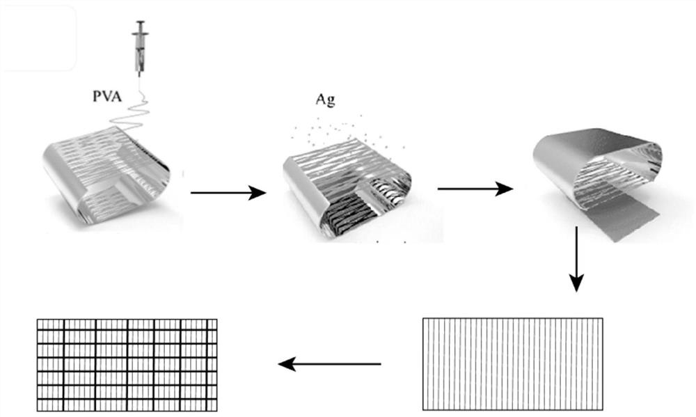
[0059] A flexible transparent conductive film with a hierarchical structure provided in this embodiment is prepared according to the following steps, as figure 2 Shown is a schematic diagram of the preparation process of the flexible transparent conductive film:
[0060] (1) The PET film with a thickness of 50 μm was washed with deionized water and absolute ethanol for 30 min, and dried as a flexible and clear substrate for future use.
[0061] (2) Three-dimensional PVA nanofiber network was prepared under the conditions of positive voltage 15kV and negative voltage 2kV by electrospinning method, and the spinning solution was PVA colloidal solution with a mass concentration of 10%.
[0062] (3) The PVA nanofiber network is placed in a magnetron sputtering apparatus to sputter metallic silver with a vacuum of 1×10 -5 Pa, the flow rate of high-purity argon is 50cm 3 / min, the distance between the target and the substrate is 6cm, the deposition beam is incident perpendicular t...
Embodiment 2
[0069] This implementation is basically the same as that of Example 1, except that in step (3), the sputtered metal is copper.
PUM
| Property | Measurement | Unit |
|---|---|---|
| thickness | aaaaa | aaaaa |
| thickness | aaaaa | aaaaa |
| thickness | aaaaa | aaaaa |
Abstract
Description
Claims
Application Information


