

Sulfide highly-uniform microsphere with precisely controllable particle size and preparing method thereof
A sulfide, precise technology, applied in chemical instruments and methods, copper sulfide, lead sulfide, etc., can solve the problems of narrow particle size range, rough control of product particle size, etc., and achieve the effect of highly uniform particle size
- Summary
- Abstract
- Description
- Claims
- Application Information
AI Technical Summary
Problems solved by technology
Method used
Image

Examples
Embodiment 1
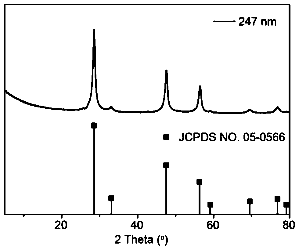
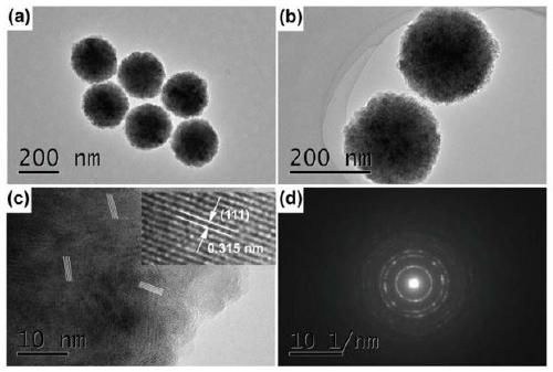
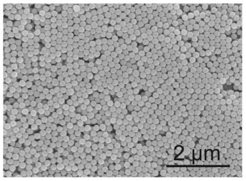
[0030] Through a multi-step growth method that accurately regulates the particle size, monodisperse ZnS nanospheres with a particle size of 235±5 nm are prepared, and three-dimensional photonic crystals are constructed using the particles of this size. The specific preparation method is:
[0031] 1) Weigh 3.00g polyvinylpyrrolidone and 100mL deionized water to fully dissolve polyvinylpyrrolidone in deionized water; obtain a uniform solution, stir and heat to 75°C; weigh 2.25g thioacetamide and add it to the reaction system; Measure 0.07mL concentrated nitric acid and add it to the reaction system; weigh 2.97g zinc nitrate hexahydrate, pre-dissolve it in 5mL deionized water, and then quickly add to the reaction system, stir vigorously at 1000rpm for 3min; reduce the stirring speed to 300 -500rpm, stirring for 2h at 75℃;
[0032] 2) Weigh 2.97g zinc nitrate hexahydrate, dissolve it in 5mL deionized water in advance, then quickly add it to a three-necked flask, stir and react in a wa...
Embodiment 2
[0039] Through a multi-step growth method that precisely regulates the particle size, monodisperse ZnS nanospheres with a particle size of 150±5 nm are prepared, and the three-dimensional photonic crystals are constructed using the particle size of the microspheres. The specific preparation method is:
[0040] 1) Weigh 3.00g polyvinylpyrrolidone and 100mL deionized water to fully dissolve polyvinylpyrrolidone in deionized water; obtain a uniform solution, stir and heat to 75°C; weigh 2.25g thioacetamide and add it to the reaction system; Measure 0.07mL concentrated nitric acid and add it to the reaction system; weigh 2.97g zinc nitrate hexahydrate, pre-dissolve it in 5mL deionized water, and then quickly add to the reaction system, stir vigorously at 1000rpm for 3min; reduce the stirring speed to 300 -500rpm, stirring for 2h at 75℃;
[0041] 2) Weigh 2.97 g of zinc nitrate hexahydrate, dissolve it in 5 mL of deionized water in advance, and then quickly add it to a three-necked fla...
Embodiment 3
[0045] Through a multi-step growth method that precisely regulates the particle size, monodisperse ZnS nanospheres with a particle size of 1000 ± 5 nm are prepared. The specific preparation method is:
[0046] 1) Weigh 3.00g polyvinylpyrrolidone and 100mL deionized water to fully dissolve polyvinylpyrrolidone in deionized water; obtain a uniform solution, stir and heat to 75°C; weigh 2.25g thioacetamide and add it to the reaction system; Measure 0.07mL concentrated nitric acid and add it to the reaction system; weigh 2.97g zinc nitrate hexahydrate, pre-dissolve it in 5mL deionized water, and then quickly add to the reaction system, stir vigorously at 1000rpm for 3min; reduce the stirring speed to 300-500rpm, stirring at 75℃ for 2h;
[0047] 2) Weigh 2.97g zinc nitrate hexahydrate, dissolve it in 5mL deionized water in advance, then quickly add it to a three-necked flask, stir and react in a water bath for 2h; weigh 2.97g zinc nitrate hexahydrate, dissolve it in 5mL deionized water...
PUM
| Property | Measurement | Unit |
|---|---|---|
| particle diameter | aaaaa | aaaaa |
| particle diameter | aaaaa | aaaaa |
| particle diameter | aaaaa | aaaaa |
Abstract
Description
Claims
Application Information