Transient adhesive tape transfer printing method without adhesion promoter

A tape, transient technology, used in semiconductor/solid-state device manufacturing, sustainable manufacturing/processing, electrical components, etc., can solve the problem of inability to accurately achieve adhesion, small adhesion switching ratio, and inability to complete transfer printing, etc. problems, to achieve the effect of improving transfer efficiency and fidelity, reducing process difficulty and cost, and enhancing reliability

Active Publication Date: 2019-06-28
西安纳智光研科技有限公司
View PDF6 Cites 4 Cited by
  • Summary
  • Abstract
  • Description
  • Claims
  • Application Information

AI Technical Summary

Problems solved by technology

However, this method has two serious defects: (1) it is difficult to accurately control the peeling rate in the two processes of "ink acquisition" and "ink release", so that the expe

Method used


Image

  • Transient adhesive tape transfer printing method without adhesion promoter

Examples


Embodiment 1

[0019] Example 1: A 200 nm thick monocrystalline silicon film was transferred by a transient adhesive tape transfer method.

[0020] Step 1, forming single crystal silicon thin film island isolation on the SOI substrate.

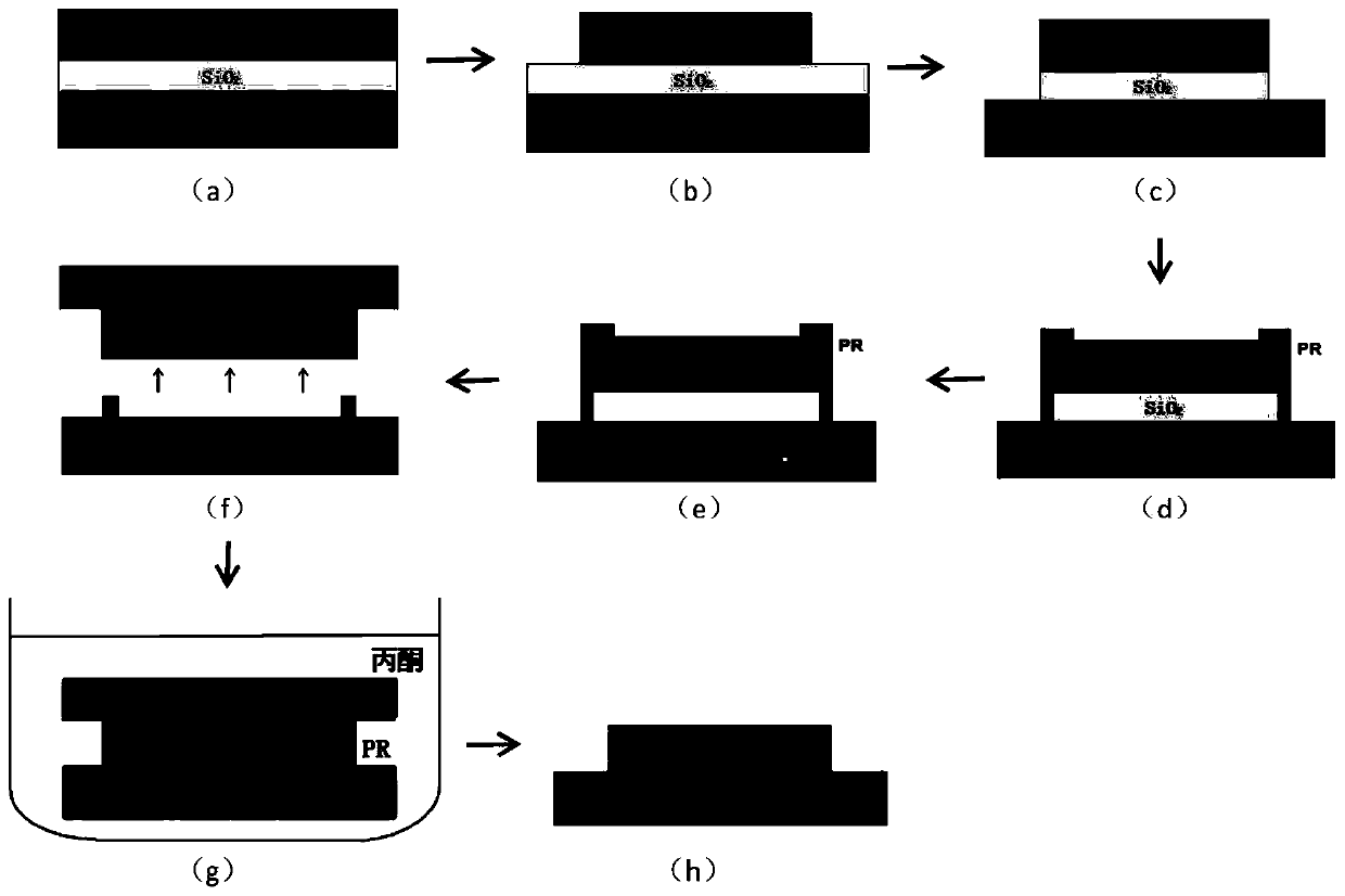
[0021] Select an SOI substrate with a single crystal silicon film thickness of 200nm and a buried oxide layer thickness of 200nm, such as figure 1 (a);

[0022] The photolithography process and reactive ion etching process are adopted, and the parameters of the etching machine used in the reactive ion etching process are set as follows: gas flow rate BCl 3 :Cl 2 =60: 60 sccm, the etching power is selected as 150W. On the upper part of the SOI substrate, monocrystalline silicon thin film islands are carved, such as figure 1 (b).

[0023] Step 2, partially etching the exposed buried oxide layer.

[0024] First, weigh 34.29 g of NH 4 F solid and 85.71ml of deionized water, mixed into 40% NH 4 F solution; then select 20ml of 40% HF solution, fully mix th...

Embodiment 2

[0036] Example 2: A 100 nm thick monocrystalline silicon film was transferred by a transient adhesive tape transfer method.

[0037] Step 1, forming single crystal silicon thin film island isolation on the SOI substrate.

[0038] Select an SOI substrate with a single crystal silicon film thickness of 100nm and a buried oxide layer thickness of 200nm, such as figure 1 (a);

[0039] The photolithography process and reactive ion etching process are adopted, and the parameters of the etching machine used in the reactive ion etching process are set as follows: gas flow rate BCl 3 :Cl 2 =60: 60 sccm, the etching power is selected as 150W. On the upper part of the SOI substrate, monocrystalline silicon thin film islands are carved, such as figure 1 (b).

[0040] Step 2, partially etching the exposed buried oxide layer.

[0041] First, first, weigh 34.29 g of NH 4 F solid and 85.71ml of deionized water, mixed into 40% NH 4 F solution; then select 20ml of 40% HF solution, fully...

Embodiment 3

[0052] Example 3: transfer a 150 nm thick monocrystalline silicon film by using a transient adhesive tape transfer method.

[0053] Step A, forming single crystal silicon thin film island isolation on the SOI substrate.

[0054] Select an SOI substrate with a single crystal silicon film thickness of 150nm and a buried oxide layer thickness of 200nm, such as figure 1 (a);

[0055] The photolithography process and reactive ion etching process are adopted, and the parameters of the etching machine used in the reactive ion etching process are set as follows: gas flow rate BCl 3 :Cl 2 =60: 60 sccm, the etching power is selected as 150W. On the upper part of the SOI substrate, monocrystalline silicon thin film islands are carved, such as figure 1 (b).

[0056] Step B, partially etching the exposed buried oxide layer.

[0057] First, weigh 34.29 g of NH 4 F solid and 85.71ml of deionized water, mixed into 40% NH 4 F solution; then select 20ml of 40% HF solution, fully mix the...


PUM

PropertyMeasurementUnit
Thicknessaaaaaaaaaa
Thicknessaaaaaaaaaa
Thicknessaaaaaaaaaa

Abstract

The invention discloses a high-efficiency and high-fidelity transient adhesive tape transfer printing method without an adhesion promoter, and mainly solves the problems of low transfer printing efficiency, low fidelity and high operation difficulty of an existing PDMS-based transfer printing technology. According to the implementation scheme, the method comprises the following steps: 1) preparinga monocrystalline silicon film on an SOI substrate; 2) preparing photoresist anchor points on the monocrystalline silicon thin film, and etching the buried oxide layer of the SOI substrate; 3) picking up a monocrystalline silicon film on the SOI substrate by using a transient adhesive tape; 4) coupling the transient adhesive tape with the monocrystalline silicon film with a receiving substrate; 5) soaking the coupled system in acetone solution, pulling out the soaked system, and drying the soaked system to remove residues dissolved in the adhesive tape, thereby completing high-efficiency andhigh-fidelity transfer printing. The method changes a traditional transfer printing mode, improves the reliability of the transfer printing technology, reduces the process difficulty and cost, achieves the higher transfer printing efficiency and fidelity, and can be used for manufacturing heterogeneous integrated chips.

Description

technical field [0001] The invention belongs to the technical field of semiconductor technology, and in particular relates to a transient adhesive tape transfer printing method without an adhesion promoter, which can be used for heterogeneous integration of devices on any substrate. technical background [0002] In the post-Moore's Law era, it has become very difficult to increase the integration level by reducing the size of transistors in the traditional way, so the concept of heterogeneous integration has gradually been valued by people. In particular, monolithic heterogeneous integration has attracted much attention, and there have been many reports explaining its development and breakthroughs. The meaning of monolithic heterogeneous integration is to integrate different materials on a single chip to manufacture various devices with different functions, so as to increase the integration degree of the chip and the functionality of the chip. For example, gallium nitride a...

Claims


Application Information

Patent Timeline
IPC IPC(8): H01L21/18
CPCY02P70/50
Inventor 张春福张家祺武毅畅陈大正张进成郝跃
Owner 西安纳智光研科技有限公司
Why Eureka
Try Eureka