

Gas sensor device, preparation method thereof and application
A gas sensor and gas-sensitive technology, applied in the field of gas sensing and sensing, can solve the problem of low sensitivity and achieve the effect of high-sensitivity sensing
- Summary
- Abstract
- Description
- Claims
- Application Information
AI Technical Summary
Problems solved by technology
Method used
Image

Examples
Embodiment 1
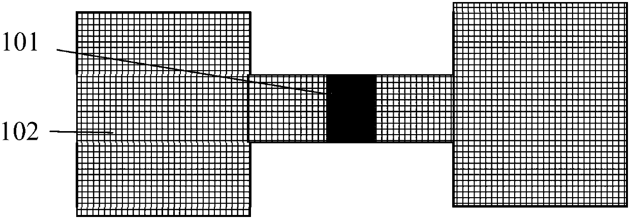
[0035] (1) On a silicon wafer with a thermally oxidized silicon dioxide film on the surface (the thickness of the silicon dioxide layer is 100-500nm), using a chemical vapor deposition method at 800-1100°C, using methane and hydrogen as reaction gases, Use argon as the carrier gas and deposit for 20 minutes to prepare graphene films with nanocrystalline structures;
[0036] (2) By spin-coating the nanocrystalline graphene film produced in step (1), 100-800nm thick electron beam sensitive photoresist is spin-coated, and the photoresist is removed by baking at 180°C for 60 seconds. Solvent, and then through electron beam direct writing, combined with oxygen plasma etching method, cut out a 5μm×5μm area on the continuous nanocrystalline graphene film to form graphene islands (that is, the gas-sensitive center section);
[0037] (3) The electrode is prepared by metal evaporation method (i.e. Figure 1a The grid area is shown): Coating photoresist (polymethyl methacrylate, PMMA) with ...
Embodiment 2
[0047] (1) On a silicon wafer with a thermally oxidized silicon dioxide film on the surface (the thickness of the silicon dioxide layer is 100-500nm), using a chemical vapor deposition method at 800-1100°C, using methane and hydrogen as reaction gases, Use argon as the carrier gas and deposit for 20 minutes to prepare graphene films with nanocrystalline structures;
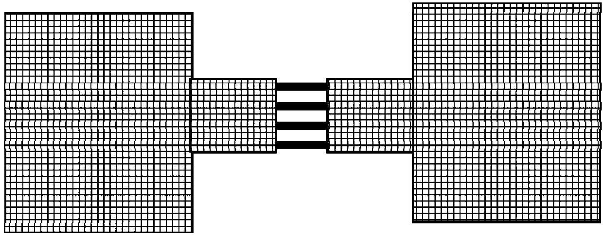
[0048] (2) By spin-coating the nanocrystalline graphene film produced in step (1), 100-800nm thick electron beam sensitive photoresist is spin-coated, and the photoresist is removed by baking at 180°C for 60 seconds. Solvent, and then through electron beam direct writing, combined with oxygen plasma etching method, cut out a 5μm×5μm area on the continuous nanocrystalline graphene film to form graphene islands (that is, the gas-sensitive center Part), and then cut the graphene island into mutually parallel strips, the width of the strip is 1 μm, and the distance between the two strips is 1 μm;
[0049] (3) The electr...
Embodiment 3
[0056] (1) On a silicon wafer with a thermally oxidized silicon dioxide film on the surface (the thickness of the silicon dioxide layer is 100-500nm), using a chemical vapor deposition method at 800-1100°C, using methane and hydrogen as reaction gases, Use argon as the carrier gas and deposit for 20 minutes to prepare graphene films with nanocrystalline structures;
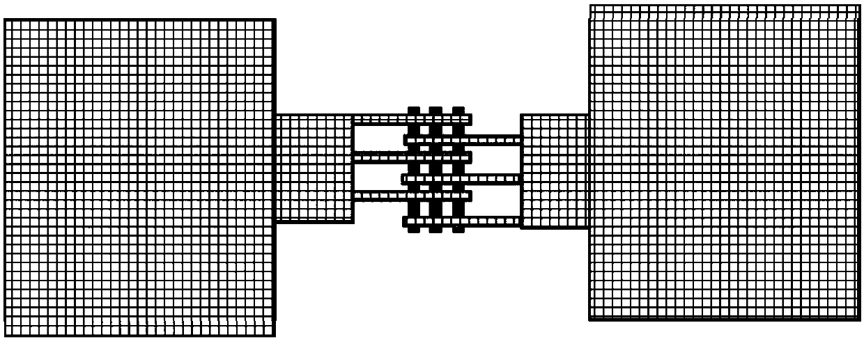
[0057] (2) By spin-coating the nanocrystalline graphene film produced in step (1), 100-800nm thick electron beam sensitive photoresist is spin-coated, and the photoresist is removed by baking at 180°C for 60 seconds. Solvent, and then through electron beam direct writing, combined with oxygen plasma etching method, cut out a 5μm×5μm area on the continuous nanocrystalline graphene film to form graphene islands (that is, the gas-sensitive center Part), and then cut the graphene island into mutually parallel strips, the width of the strip is 1 μm, and the distance between the two strips is 1 μm;
[0058] (3) The electr...
PUM
| Property | Measurement | Unit |
|---|---|---|
| Thickness | aaaaa | aaaaa |
Abstract
Description
Claims
Application Information