

Diode device and manufacturing process thereof
A manufacturing process and diode technology, applied in semiconductor/solid-state device manufacturing, semiconductor devices, electrical components, etc., can solve the problem of low reverse withstand voltage, and achieve the effect of low on-voltage
- Summary
- Abstract
- Description
- Claims
- Application Information
AI Technical Summary
Problems solved by technology
Method used
Image

Examples
Embodiment approach
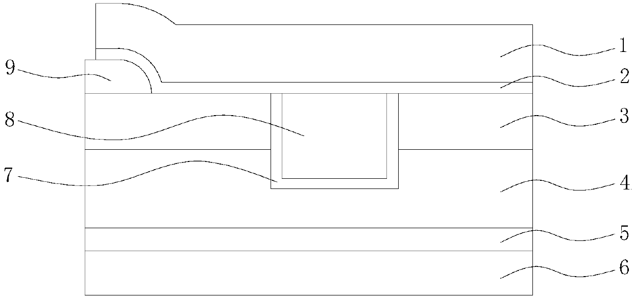
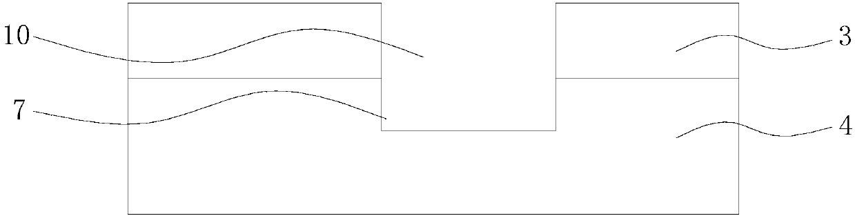
[0054] Furthermore, please also refer to figure 1 and Figure 7-10 , as a specific embodiment of the diode device provided by the present invention, it also includes a dielectric oxide layer 9 located at one end of the P-type doped region 3, and the dielectric oxide layer 9 is arranged between the barrier layer 2 and the P-type doped region 3 space, and a part of the dielectric oxide layer 9 is exposed to the air. The arrangement of the dielectric oxide layer 9 improves the reverse withstand voltage capability of the diode device, and can prevent external foreign matter from invading into the diode device to protect the diode device.
[0055] Please also refer to Figure 1-10 , the manufacturing process of the diode device provided by the present invention will now be described. A manufacturing process for a diode device, comprising the following steps:
[0056] S1. Prepare N-type lightly doped region 4;
[0057] S2, forming a P-type doped region 3 on the N-type lightly ...
specific Embodiment approach
[0070] Further, see figure 2 , as a specific implementation of the manufacturing process of the diode device provided by the present invention, step S2 includes:
[0071] The P-type doped region 3 is formed by ion implantation on the wafer, by diffusion on the furnace tube or by vapor phase epitaxy on the N-type lightly doped region 4 .
[0072] Tight integration can be achieved between the P-type doped region 3 and the N-type lightly doped region 4 formed by ion implantation, by diffusion on the furnace tube or by vapor phase epitaxy, so that the electrons in the P-type The movement between the doped region 3 and the N-type lightly doped region 4 is more sufficient.
[0073] Specifically, the setting of the concentration of the P-type doped region 3 will enable electrons to accumulate around the oxide layer 7, and the P-type doped region 3 will also be able to form a Schottky contact with the barrier layer 2, thereby improving the efficiency of the diode device. reverse wi...
PUM
 Abstract
Description
Claims
Application Information