Manufacturing method of full-color Micro-LED display device based on quantum dot photo-conversion layer

A light conversion layer and display device technology, applied in the direction of electric solid-state devices, semiconductor devices, electrical components, etc., can solve problems such as optical crosstalk, light source arrays and quantum dot film layers are tightly adhered and difficult to separate, so as to improve utilization rate, Filter out harmful spectral components to the human eye and avoid cross-linking effects

Active Publication Date: 2019-07-05
CHANGCHUN INST OF OPTICS FINE MECHANICS & PHYSICS CHINESE ACAD OF SCI
View PDF1 Cites 34 Cited by
  • Summary
  • Abstract
  • Description
  • Claims
  • Application Information

AI Technical Summary

Problems solved by technology

[0006] The present invention solves the problem that the existing quantum dot materials are directly coated on the surface of the Micro-LED. After the coating process is completed, the quantum dot materials above the adjacent pixel units will diffuse laterally during the low-temperature thermal annealing process, and the mixing of dif

Method used


Image

  • Manufacturing method of full-color Micro-LED display device based on quantum dot photo-conversion layer
  • Manufacturing method of full-color Micro-LED display device based on quantum dot photo-conversion layer
  • Manufacturing method of full-color Micro-LED display device based on quantum dot photo-conversion layer

Examples


specific Embodiment approach 1

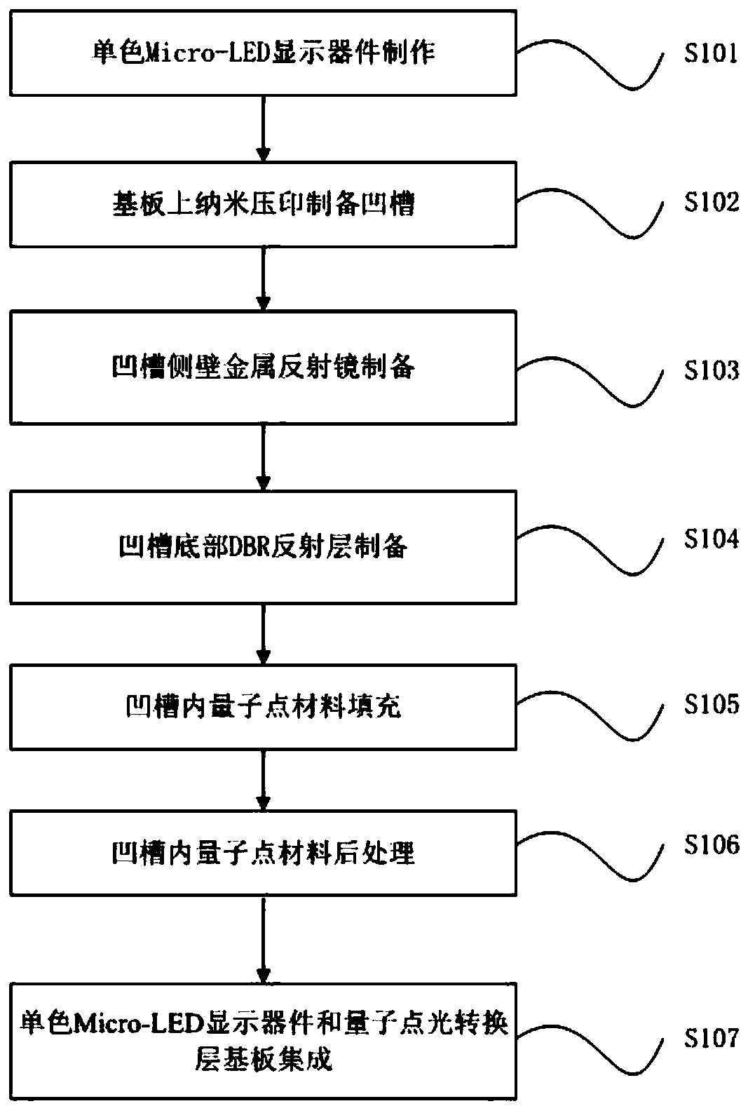
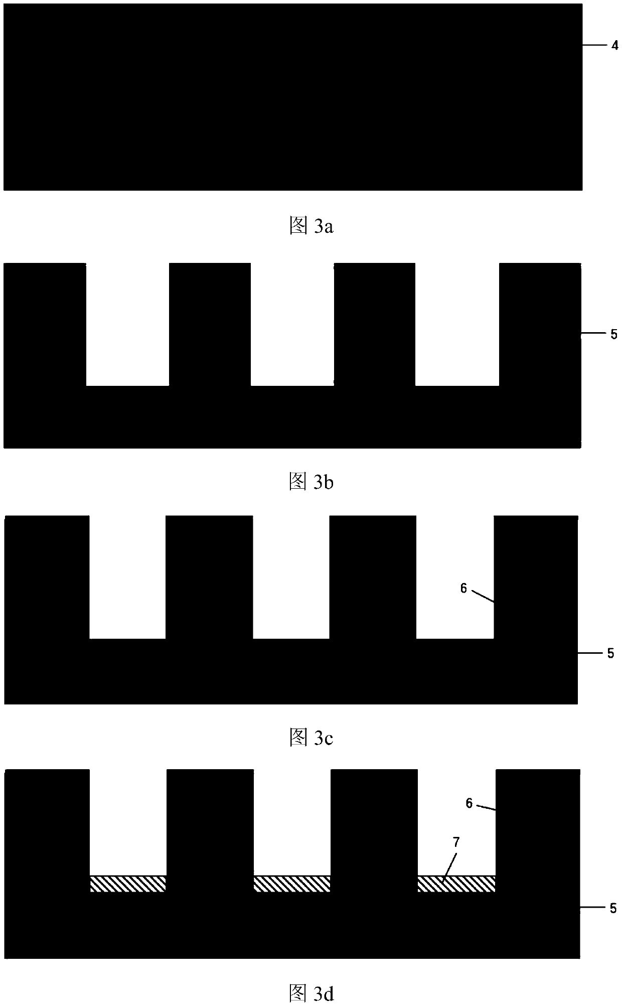
[0025] Specific implementation mode 1. Combination Figure 1 to Figure 4 Describe this embodiment, the fabrication method of the full-color Micro-LED display device based on the quantum dot light conversion layer, the method is realized by the following steps:

[0026] Step S101: Provide a blue LED epitaxial wafer with a sapphire substrate 17, a Si-based CMOS passive drive backplane, and manufacture a monochrome Micro-LED display device;

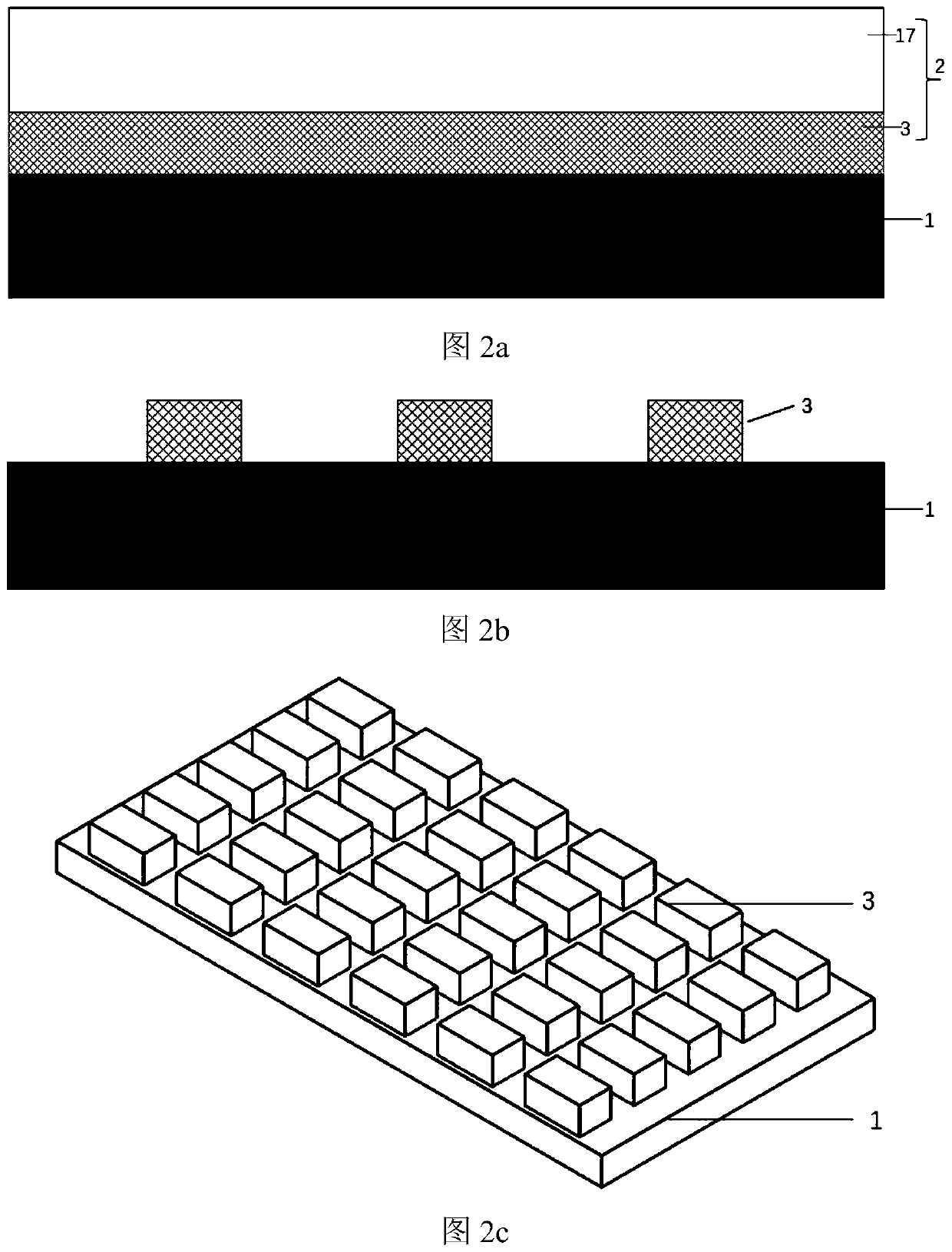
[0027] combine figure 2 a, after the GaN-based LED epitaxial wafer 2 on the sapphire substrate 17 and the Si-based CMOS active driving backplane 1 are bonded at the wafer level, after the sapphire substrate 17 is lifted off by laser, a single pixel can be prepared by ICP etching and other technologies Single-color Micro-LED array driven by independent addressing3, figure 2 b is a cross-sectional view of a monochromatic Micro-LED array, figure 2 c is the top view of the monochromatic Micro-LED array.

[0028] The preparation of the mon...


PUM


Abstract

The invention discloses a manufacturing method of a full-color Micro-LED display device based on a quantum dot photo-conversion layer, and relates to the technical field of preparation of displays. The following problems are solved: existing quantum dot materials are directly coated with the surface of Micro-LED, and after a coating process is completely carried out, the quantum dot materials arranged above adjacent pixel units can be horizontally diffused in a low-temperature heat annealing process, and serious optical crosstalk interference can be caused by mixing the different quantum dot materials. Light source arrays are tightly adhered with quantum dot film layers so that difficult separation between the light source arrays and the quantum dot film layers is achieved; a photo-conversion layer base plate is prepared by coating quantum dot material subareas of different colors with different positions of glass or polymer base plates; a monochromatic Micro-LED display array is adhered with the photo-conversion base plate, so that full-color display of the Micro-LED is realized. A DBR reflective mirror is prepared at the bottom of a groove so as to inhibit emission of the monochromatic Micro-LED display array, so that a light source utilization ratio is increased. The full-color Micro-LED display device prepared by adopting the method has the advantages of less optical crosstalk interference of the adjacent pixels, high utilization ratio of excitation light sources and high display quality.

Description

technical field [0001] The invention relates to the technical field of display preparation, in particular to a full-color Micro-LED display device based on a quantum dot light conversion layer and a manufacturing method thereof. Background technique [0002] Micro-LED is the latest achievement of further miniaturization of traditional LED with the continuous development of micro-nano processing technology in recent years. The size of the light-emitting unit of traditional LED is usually larger than 100 μm, while the size of a single Micro-LED is less than 100 μm. The Micro-LED display device is a two-dimensional array display device composed of high-density pixel light-emitting units integrated on a single chip. Compared with LCD and OLED display devices, Micro-LED display devices have advantages in power consumption, service life, responsiveness, and viewing angle, and also have a display quality that is superior to LCD and close to OLED. [0003] At present, there are man...

Claims


Application Information

Patent Timeline
IPC IPC(8): H01L27/15H01L33/50
CPCH01L27/156H01L33/508H01L2933/0041
Inventor 王惟彪王家先梁静秋陶金李阳赵永周吕金光秦余欣王浩冰
Owner CHANGCHUN INST OF OPTICS FINE MECHANICS & PHYSICS CHINESE ACAD OF SCI
Why Eureka
Try Eureka