

QLED device
A technology of devices and quantum dot materials, applied in the field of QLED devices, can solve problems affecting the luminous purity and recombination efficiency of quantum dot light-emitting devices, affecting the luminous characteristics of quantum dots, etc.
- Summary
- Abstract
- Description
- Claims
- Application Information
AI Technical Summary
Problems solved by technology
Method used
Image


Examples
Embodiment 1
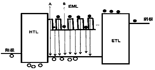
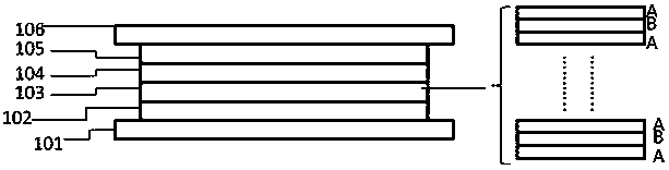
[0034] The structure of the QLED device in this embodiment is: an ITO anode layer, a PEDOT:PSS hole injection layer, a TFB hole transport layer, a [ZnSCdSZnS] light-emitting layer, a ZnO electron transport layer and an Al cathode layer are sequentially stacked on a glass substrate.
[0035] The preparation method of the QLED device in this embodiment is as follows:
[0036] a. Spin-coat one deck of PEDOT on ITO substrate:PSS thin film is used as hole injection layer;
[0037] b. Spin-coat a layer of TFB film on the PEDOT:PSS layer as a hole transport layer;
[0038] c. Deposit a quantum dot light-emitting layer based on a single-band difference superlattice structure by magnetron sputtering, wherein the quantum dot light-emitting layer is a three-layer single-band difference superlattice energy level structure functional layer, including sequentially arranged ZnSCdSZnS, with a thickness of 50nm, in which, the thickness of ZnS on both sides is 5nm, and the thickness of CdS in ...
Embodiment 2
[0042] The structure of the QLED device in this embodiment is: an ITO anode layer, a PEDOT:PSS hole injection layer, a TFB hole transport layer, a [ZnSCdSZnS]2 light-emitting layer, a ZnO electron transport layer and an Al cathode layer formed sequentially on a glass substrate .
[0043] The preparation method of the QLED device in this embodiment is as follows:
[0044] a. Spin-coat one deck of PEDOT on ITO substrate:PSS thin film is used as hole injection layer;
[0045] b. Spin-coat a layer of TFB film on the PEDOT:PSS layer as a hole transport layer;
[0046] c. Deposit a quantum dot light-emitting layer based on a single-band difference superlattice structure by magnetron sputtering, wherein the quantum dot light-emitting layer is a six-layer single-band difference superlattice energy level structure functional layer, including sequentially arranged [ZnSCdSZnS]2, the thickness is 40nm, in which, the thickness of ZnS on both sides is 5nm, and the thickness of CdS in the ...
Embodiment 3
[0050] The structure of the QLED device in this embodiment is: an ITO anode layer, a PEDOT:PSS hole injection layer, a TFB hole transport layer, a [ZnSCdSZnS]2 light-emitting layer, a ZnO electron transport layer and an Al cathode layer formed sequentially on a glass substrate .
[0051] The preparation method of the QLED device in this embodiment is as follows:
[0052] a. Spin-coat one deck of PEDOT on ITO substrate:PSS thin film is used as hole injection layer;
[0053] b. Spin-coat a layer of TFB film on the PEDOT:PSS layer as a hole transport layer;
[0054] c. Deposit a quantum dot light-emitting layer based on a single-band difference superlattice structure by magnetron sputtering, wherein the quantum dot light-emitting layer is a six-layer single-band difference superlattice energy level structure functional layer, including sequentially arranged [ZnSCdSZnS]2, the thickness is 36nm, in which, the thickness of ZnS on both sides is 4nm, and the thickness of CdS in the ...
PUM
| Property | Measurement | Unit |
|---|---|---|
| Luminescence spectrum | aaaaa | aaaaa |
| Luminescence spectrum | aaaaa | aaaaa |
| Thickness | aaaaa | aaaaa |
Abstract
Description
Claims
Application Information