Modulation method of drain electrode power supply modulation chip of GaN power amplifier

A power amplifier and power modulation technology, applied in power amplifiers, amplifier protection circuit layout, amplifiers, etc., can solve problems such as large static power consumption, period damage, timing errors, etc., achieve large input current, increase power capacity, and reduce decline. Effects along time

Inactive Publication Date: 2019-07-05
南京固德芯科技有限公司
View PDF6 Cites 12 Cited by
  • Summary
  • Abstract
  • Description
  • Claims
  • Application Information

AI Technical Summary

Problems solved by technology

[0006] Aiming at the problems existing in the prior art that are easy to cause timing errors, cause damage during the period, and have high static power consumption, the present invention provides a modulation method for the GaN power amplifier drain power modulation chip, which can realize the stability of the power amplifier when it is powered on. , and the GaN power amplifier has low static power consumption

Method used


Image

  • Modulation method of drain electrode power supply modulation chip of GaN power amplifier
  • Modulation method of drain electrode power supply modulation chip of GaN power amplifier
  • Modulation method of drain electrode power supply modulation chip of GaN power amplifier

Examples


Embodiment 1

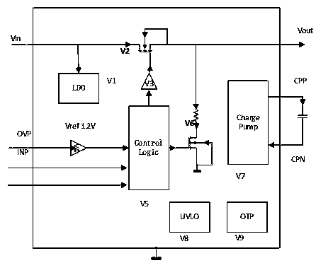
[0036] The purpose of the present invention is to solve the problem of device damage caused by wrong power-on sequence of the GaN power amplifier and the large static power consumption of the GaN power amplifier, and proposes a drain-level power supply modulation chip of the GaN power amplifier.

[0037] Such as figure 1 As shown, including: linear voltage regulator, the V1 linear voltage regulator in the figure is used to convert the input high voltage into the low voltage required by the internal control circuit. After the linear voltage regulator converts the input voltage from the VIN terminal of the chip, the low voltage is supplied to internal devices, and the output terminal of the linear voltage regulator is connected to the corresponding VLDO terminal of the chip.

[0038] The high-power N-channel switch tube V2 uses an N-channel MOSFET as a high-power switch tube; the drain input of V2 is the constant voltage VIN input by the chip. The source output is a pulse modul...

Embodiment 2

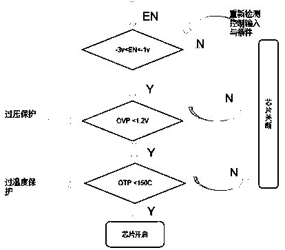
[0050] The control logic flow chart of the control method of the power modulation chip of this scheme is shown in figure 2 .

[0051] After the chip is powered on, it will first detect whether there is a negative voltage input of -3V to -1V on the EN pin. If there is, it will start to detect whether the voltage of the OPV input pin after the external voltage dividing resistor is less than 1.2V. If there is no voltage in this range, re-detect the EN pin input;

[0052] If the voltage of the OPV input pin is less than 1.2V, continue to detect whether the chip junction temperature is lower than 150°C. If it is not less than 1.2V, the chip returns to re-detect the EN pin voltage;

[0053] If the chip junction temperature is lower than 150°C, the chip is turned on. The chip junction temperature is not lower than 150°C, and the chip returns to retest the EN pin voltage;

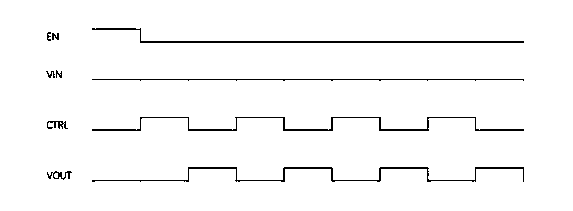
[0054] The external constant DC high voltage input enters the chip through the VIN pin. The CTRL signal is...


PUM


Abstract

The invention discloses a modulation method of a drain electrode power supply modulation chip of a GaN power amplifier, and belongs to the field of chip design. The modulation method of a drain electrode power supply modulation chip of a GaN power amplifier comprises a linear voltage stabilizer, a comparator, a charge pump, a high-power N-channel switch tube, a negative electricity detection control unit, an over-temperature and over-voltage protection unit, a power supply modulation unit and an output rapid discharge channel. On-off of drain electrode input of the GaN power amplifier is controlled by detecting whether negative voltage exists in a grid electrode of the GaN power amplifier or not, and therefore power supply time sequence control over the GaN power amplifier is achieved. On-off of the switch tube is controlled by controlling the gate-source voltage of the power switch tube in the chip, so that pulse modulation of drain electrode power supply of the GaN power amplifier isrealized. The design of a monolithic integrated circuit is adopted, so that the hardware layout area is reduced; while integrating the drain electrode modulation function, the invention also providesa perfect GaN power amplifier protection function, including drain electrode negative pressure enabling and over-temperature and over-voltage protection.

Description

technical field [0001] The invention relates to the field of chip design, more specifically, to a modulation method of a GaN power amplifier drain power modulation chip. Background technique [0002] Due to its high energy density and high operating frequency, the GaN power amplifier has become an indispensable power amplifier device for the new generation of active phased array radar. Since the active phased array radar uses a pulse signal, there is no signal transmission for most of the time in a pulse period. Through the drain modulation, the static power consumption of the GaN power amplifier can be greatly reduced, the system efficiency can be improved and the transmission noise can be reduced. At the same time, since the GaN power amplifier is a depletion-type device, the drain voltage must be switched under the condition of negative gate voltage, otherwise the device will be burned, so the control of the power-on sequence is also particularly important. [0003] The ...

Claims


Application Information

Patent Timeline
Patent Type & Authority Applications(China)
IPC IPC(8): H03F1/02H03F1/52H03F3/21
CPCH03F1/0211H03F1/523H03F3/21
Inventor 徐步黎遥
Owner 南京固德芯科技有限公司
Why Eureka
Try Eureka