
A kind of composite material and its preparation method and application

A technology of composite materials and prefabricators, applied in semiconductor/solid-state device manufacturing, semiconductor devices, electrical components, etc., can solve problems such as low efficiency and lifespan, unbalanced carrier injection, and high preparation costs

Active Publication Date: 2021-04-09
TCL CORPORATION
View PDF3 Cites 0 Cited by
  • Summary
  • Abstract
  • Description
  • Claims
  • Application Information

AI Technical Summary

Problems solved by technology

[0005] The purpose of the present invention is to provide a composite material and its preparation method and application, aiming to solve the problems of low efficiency, lifespan and high preparation cost of existing blue light devices due to carrier injection imbalance

Method used


Image

  • A kind of composite material and its preparation method and application

Examples


preparation example Construction

[0025] The embodiment of the present invention provides the preparation method of the composite material corresponding to the previous embodiment. This preparation method comprises the steps:

[0026] Step S11: BiOI is provided, and the surface of BiOI is modified by a coupling agent to obtain modified BiOI.

[0027] In the embodiment of the present invention, in order to improve the compatibility between the polymer and the BiOI particles, the surface is first modified with a coupling agent to promote the subsequent combination of the BiOI particles and PMMA; the coupling agent is specifically a silane coupling agent , which can be methacryloxypropyltrimethoxysilane (MPS), 3-aminopropyltriethoxysilane (APTES) or other silane coupling agents, so that the alkoxy groups it has directly bond with BiOI The hydroxyl groups on the surface react to graft onto the surface of BiOI particles to achieve the purpose of modification.

[0028] Step S12: Disperse the modified BiOI in a pol...

Embodiment 1

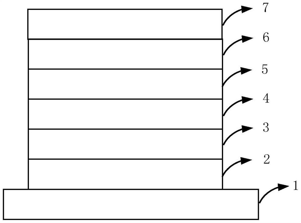
[0079] (1) First, place the patterned ITO substrate in acetone, lotion, deionized water, and isopropanol in order for ultrasonic cleaning, and each step of ultrasonic cleaning needs to last for about 15 minutes. After the ultrasound is completed, place the ITO in a clean oven to dry for later use.

[0080] (2) After the ITO substrate was dried, the ITO surface was treated with UV-ozone for 5 minutes to further remove the organic matter attached to the ITO surface and improve the work function of the ITO.

[0081] (3) Print a layer of PEDOT:PSS on the surface of the treated ITO substrate with a thickness of 30nm, and heat the substrate on a heating table at 150°C for 30 minutes to remove moisture. This step needs to be completed in air.

[0082] (4) Place the dried substrate coated with the hole injection layer in a nitrogen atmosphere, print a layer of hole transport layer material TFB, the thickness of this layer is 30nm, and then vacuumize under 10pa pressure for 30min to re...

Embodiment 2

[0087] (1) Place the patterned ITO substrate in acetone, lotion, deionized water and isopropanol in sequence for ultrasonic cleaning, and each step of ultrasonic cleaning needs to last for about 15 minutes. After the ultrasound is completed, place the ITO in a clean oven to dry for later use.

[0088] (2) After the ITO substrate was dried, the ITO surface was treated with UV-ozone for 5 minutes to further remove the organic matter attached to the ITO surface and improve the work function of the ITO.

[0089] (3) Spin-coat a layer of PEDOT:PSS on the surface of the treated ITO substrate with a thickness of 30nm, and place the substrate on a heating table at 150°C for 30 minutes to remove moisture. This step needs to be completed in air.

[0090] (4) Place the dried substrate coated with the hole injection layer in a nitrogen atmosphere, spin coat a layer of hole transport layer material PVK, the thickness of this layer is 30nm, and place it on a heating stage at 150°C Heat for...


PUM

PropertyMeasurementUnit
thicknessaaaaaaaaaa
thicknessaaaaaaaaaa
thicknessaaaaaaaaaa

Abstract

The invention belongs to the field of display devices and provides a composite material, a preparation method and application thereof. The PMMA-coated BiOI composite material provided by the present invention combines the characteristics of the two materials, so that the balance of electrons and holes can be adjusted. The electrons transition from the valence band to the conduction band, generating electron-hole pairs; on the other hand, the core BiOI has a unique layered structure, so that the corresponding atoms and atomic orbitals have enough space to be polarized, which can effectively realize the photogenerated electron- The separation of hole pairs; at the same time, BiOI is an indirect band gap compound, and the excited electrons cannot directly return to the valence band, which inhibits the recombination of electrons and holes; and the PMMA shell layer can effectively block the photogenerated electrons with lower energy. The photogenerated electrons with higher energy escape.

Description

technical field [0001] The invention belongs to the field of display devices, and in particular relates to a composite material and its preparation method and application. Background technique [0002] Quantum dot materials have the advantages of high light color purity, high luminous quantum efficiency, adjustable luminous color, high quantum yield, etc., and can be used in printing process preparation, so quantum dot-based light-emitting diodes (Quantum Dot Light Emitting Diode, QLED ) has received widespread attention recently, and its device performance indicators have also developed rapidly. [0003] At present, although the efficiency and lifespan of existing QLED devices have been greatly improved through the improvement of quantum dot materials and the continuous optimization of the structure of QLED devices, their efficiency is still far from the requirements of industrial production. Among them, the unbalanced carrier injection is a main reason affecting the devic...

Claims


Application Information

Patent Timeline
Patent Type & Authority Patents(China)
IPC IPC(8): H01L51/50H01L51/54H01L51/56
CPCH10K50/18H10K71/00
Inventor 李龙基曹蔚然
Owner TCL CORPORATION
Learn More