Semiconductor device manufacturing method

A manufacturing method and semiconductor technology, applied in the direction of semiconductor/solid-state device manufacturing, semiconductor devices, transistors, etc., can solve the problems of lowering and electron beam irradiation on the first main surface side, and achieve low recovery loss Effect

Active Publication Date: 2019-07-09
SHINDENGEN ELECTRIC MFG CO LTD
View PDF9 Cites 2 Cited by
  • Summary
  • Abstract
  • Description
  • Claims
  • Application Information

AI Technical Summary

Problems solved by technology

[0008] However, in the conventional manufacturing method of a semiconductor device, since charges are generated on the gate insulating film 922 during the electron beam irradiation process, the gate insulating film 922 is usually charged, resulting in a threshold voltage V TH get lower
And this kind of situation not only occurs when the electron beam is irradiated from the second main surface side, but also may occur when the electron beam is irradiated from the first main surface side.

Method used


Image

  • Semiconductor device manufacturing method
  • Semiconductor device manufacturing method
  • Semiconductor device manufacturing method

Examples


Embodiment approach 1

[0046] 1. Configuration of the semiconductor device 100 in the first embodiment

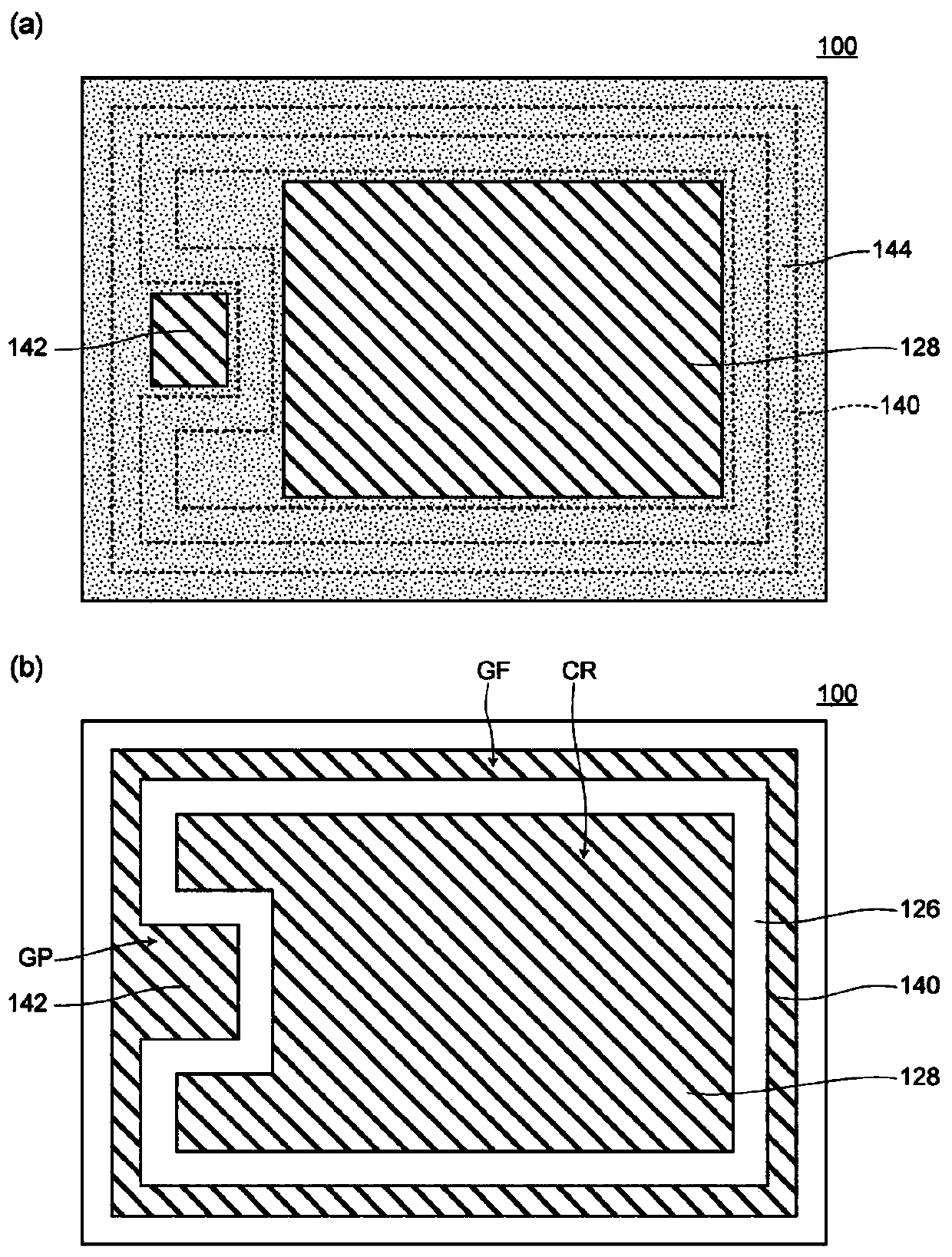
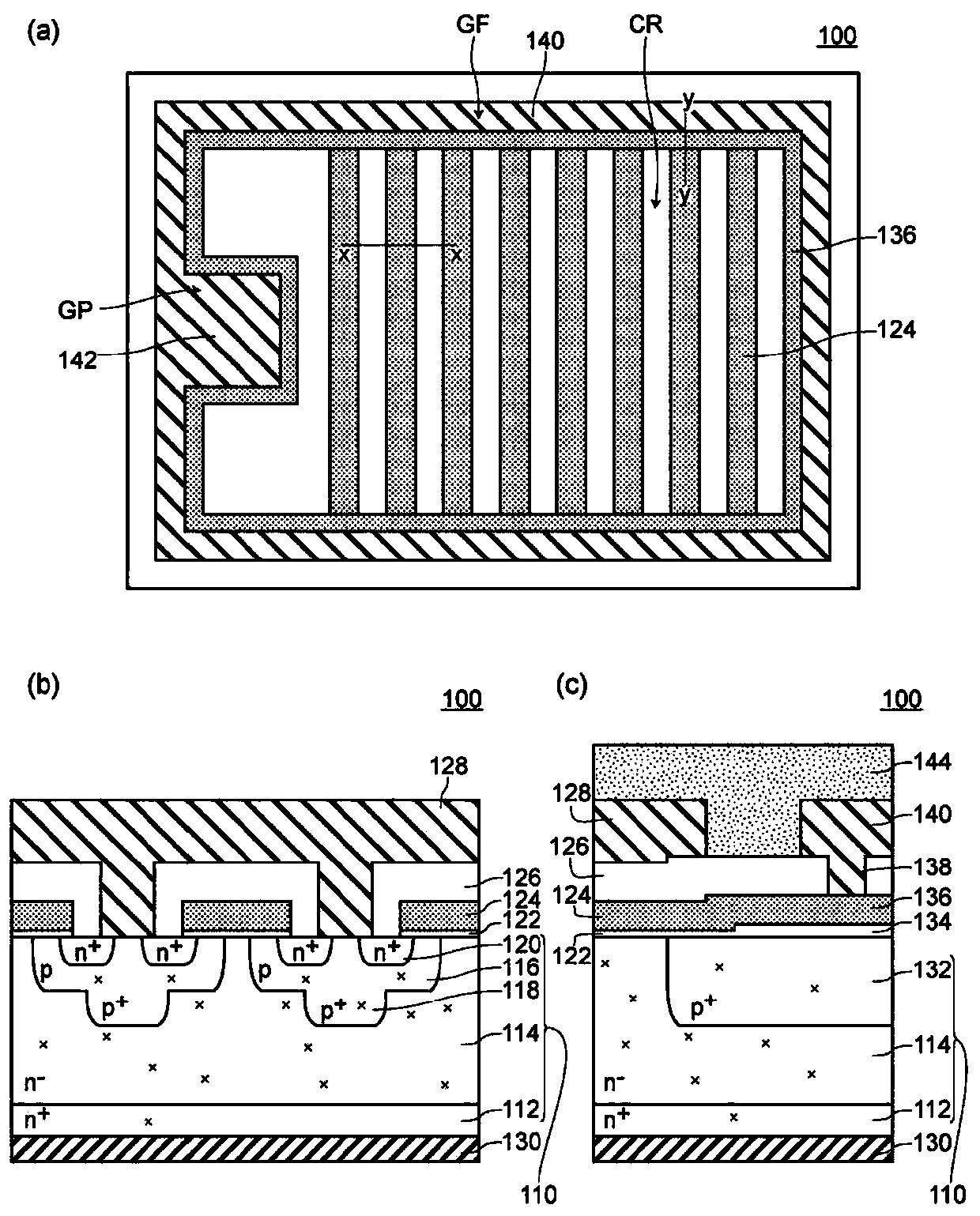
[0047] The semiconductor device 100 in Embodiment 1 is a planar semiconductor device (MOSFET) (refer to figure 2 ), which includes: are delineated in the stack with n + type low resistance semiconductor layer 112 with n - The cell region CR on the semiconductor substrate 110 of the type drift layer 114; and the peripheral region defined around the cell region CR. The peripheral region is composed of a gate wiring formation region GF surrounding the cell region CR, and a gate pad formation region GP protruding toward the cell region CR (inwardly) (refer to figure 1 (b) and figure 2 ).

[0048] The active electrode 128 is formed on the surface of the first main surface of the semiconductor substrate 110 in the cell region CR (refer to figure 1 (b)). In addition, a gate wiring 140 (gate finger) is formed on the surface of the first main surface of the semiconductor base 110 in the gate wir...

Embodiment approach 2

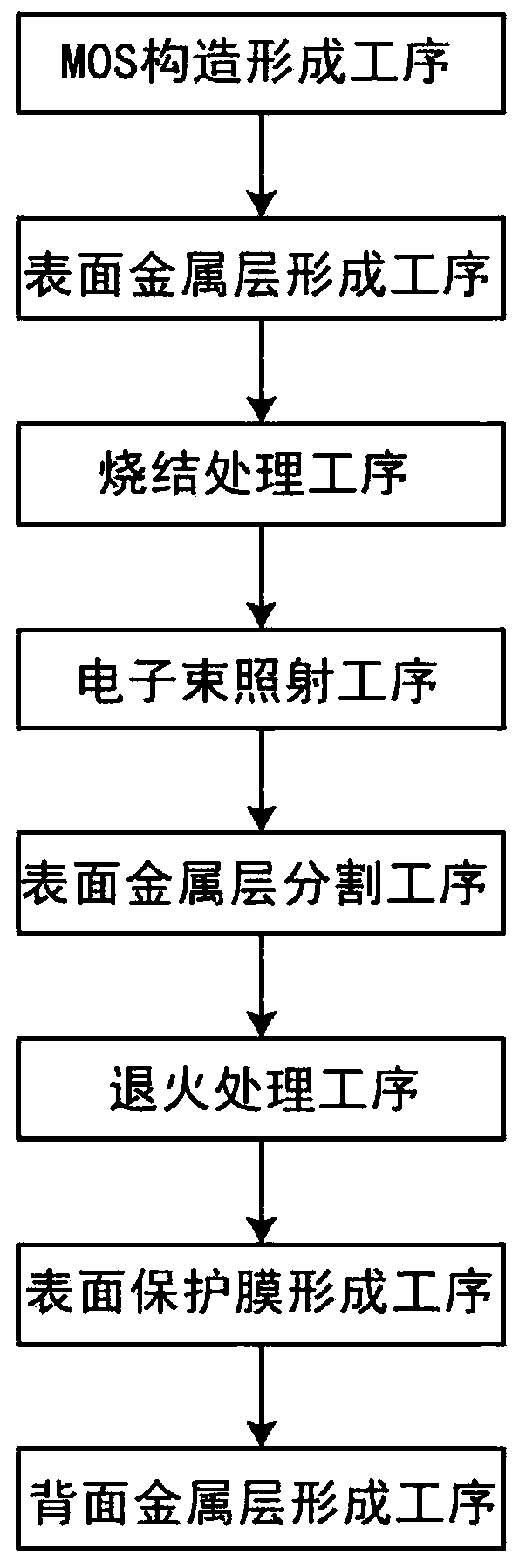
[0107] Although the manufacturing method of the semiconductor device in Embodiment Mode 2 includes basically the same steps as the manufacturing method of the semiconductor device in Embodiment Mode 1, it manufactures trench gate MOSFETs instead of planar gate MOSFETs. This point is different from the method of manufacturing the semiconductor device in Embodiment 1. like Figure 11 As shown, in the manufacturing method of the semiconductor device in the second embodiment, the semiconductor base 110 has in the cell region CR: a low-resistance semiconductor layer 112, a drift layer 114, and a p-type base region formed on the surface of the drift layer 114 116, and the source region 120 arranged in the base region 116 and formed so that at least a part is exposed on the inner peripheral surface of the trench 150 described later, the semiconductor device 102 has a first On the main surface side, the base region 116 is opened and reaches the plurality of trenches 150 of the drift ...


PUM


Abstract

A semiconductor device manufacturing method of the present invention is characterized by comprising, in this order: a MOS structure forming step of forming a gate electrode on a first major surface side of a semiconductor substrate with a gate insulating film interposed therebetween, and then forming an interlayer insulating film so as to cover the gate electrode; a metal layer forming step of forming, over the interlayer insulating film, a metal layer in a state of being connected to the gate electrode; an electron beam irradiating step of irradiating the semiconductor substrate with an electron beam in a state in which the metal layer is at ground potential, to thereby generate a lattice defect in the semiconductor substrate; a metal layer dividing step of dividing the metal layer into aplurality of electrodes; and an anneal processing step of heating the semiconductor substrate to repair the lattice defect in the semiconductor substrate. In a MOSFET according to the present invention, a parasitic internal diode recovery loss can be reduced compared with when the electron beam irradiating step is not implemented, and the semiconductor device manufacturing method provided makes it possible to manufacture a semiconductor device having a VTH characteristic comparable to that when the electron beam irradiating step is not implemented.

Description

technical field [0001] The present invention relates to a method of manufacturing a semiconductor device. Background technique [0002] Conventionally, a method of manufacturing a semiconductor device including a step of introducing lattice defects into the semiconductor substrate after irradiating the semiconductor substrate with electron beams has been widely known (for example, refer to Patent Document 1). [0003] Conventional semiconductor device manufacturing methods such as Figure 17 As shown, it includes in sequence: a MOS structure forming process, a surface metal layer forming process, a patterning process, an electron beam irradiation process, and an annealing process. That is, it includes sequentially: a MOS structure forming step, after forming the gate electrode 924 on the first main surface side of the semiconductor substrate 910 through the gate insulating film 922, forming an interlayer insulating film 926 to cover the gate electrode 924 (refer to Figure ...

Claims


Application Information

Patent Timeline
Patent Type & Authority Applications(China)
IPC IPC(8): H01L21/336H01L21/322H01L29/78
CPCH01L21/263H01L21/02H01L29/66333H01L29/66348H01L29/66712H01L29/66734H01L29/78H01L29/7802H01L29/7813H01L29/7395H01L29/7397H01L29/4238H01L29/0619H01L21/324H01L29/401
Inventor 宫腰宣树
Owner SHINDENGEN ELECTRIC MFG CO LTD
Why Eureka
Try Eureka