Supercharge Your Innovation With Domain-Expert AI Agents!

Transparent conductive film and manufacturing method thereof

A technology of transparent conductivity and manufacturing method, which is applied in the direction of cable/conductor manufacturing, chemical instruments and methods, conductive layers on insulating carriers, etc., can solve problems such as rise in resistivity, damage to ITO layer characteristics, etc., and achieve excellent crack resistance Effect

Inactive Publication Date: 2019-07-19
NITTO DENKO CORP
View PDF4 Cites 4 Cited by
  • Summary
  • Abstract
  • Description
  • Claims
  • Application Information

AI Technical Summary

Problems solved by technology

When cracks are formed on the surface of the ITO layer, the resistivity increases significantly, impairing the properties of the ITO layer

Method used


Image

  • Transparent conductive film and manufacturing method thereof
  • Transparent conductive film and manufacturing method thereof
  • Transparent conductive film and manufacturing method thereof

Examples


Embodiment 1

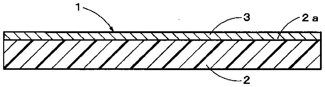
[0076] (polymer film substrate)

[0077] As the polymer film substrate, a polyethylene terephthalate (PET) film of O300E (thickness 125 μm) manufactured by Mitsubishi Plastics Corporation was used.

[0078] (Formation of organic dielectric layer)

[0079] A thermosetting resin composition containing a melamine resin: an alkyd resin: an organosilane condensate in a weight ratio of 2:2:1 in terms of solid content was diluted with methyl ethyl ketone so that the solid content concentration became 8% by weight. The obtained diluted composition was applied to one main surface of the film while conveying the PET film roll-to-roll, and heat-cured at 150° C. for 2 minutes to form an organic dielectric layer with a film thickness of 35 nm.

[0080] (degassing treatment)

[0081] The obtained PET film with an organic dielectric layer was installed in a vacuum sputtering device, and was wound up while the film was advanced in close contact with a heated film-forming roll. While moving...

Embodiment 2

[0087] A transparent conductive film was obtained in the same manner as in Example 1, except that a single-layer transparent conductive layer having a thickness of 25 nm was formed using a target having a tin oxide concentration of 10% by weight of ITO.

Embodiment 3

[0089] A transparent conductive film was obtained in the same manner as in Example 2 except that the organic dielectric layer was not formed on the polymer film substrate.


PUM

PropertyMeasurementUnit
electrical resistivityaaaaaaaaaa

Abstract

Provided are a transparent conductive film having features that a transparent conductive layer has a low specific resistance and a small thickness, while having an excellent crack resistance, and a manufacturing method thereof. A transparent conductive film (1) in the embodiment includes a polymeric film substrate (2) and a transparent conductive layer (3) formed on the main surface (2a) of the polymeric film substrate (2). The transparent conductive film (1) can have an elongated shape and is wound into a roll. The transparent conductive layer (3) is a crystalline transparent conductive layer comprising an indium tin composite oxide, has a residual stress of less than or equal to 600 MPa, has a specific resistance of 1.1*10-4 [omega].cm to 3.0*10-4 [omega].cm, and has a thickness of 15 nm to 40 nm.

Description

[0001] This application is a divisional application with an application date of May 15, 2015, an application number of 201580002175.9, and an invention title of transparent conductive film and its manufacturing method. technical field [0002] The present invention relates to a transparent conductive film having a crystalline transparent conductive layer on a polymer film substrate and a method for producing the same. Background technique [0003] A transparent conductive film in which a transparent conductive layer such as an ITO layer (indium tin composite oxide layer) is formed on a polymer film substrate is widely used in touch panels and the like. In recent years, along with the increase in screen size and thickness of panels, the ITO layer has been required to further reduce the resistivity and reduce the thickness. [0004] In a thin ITO layer, in order to secure the same surface resistance value as that of conventional ITO layers, it is necessary to increase the crys...

Claims


Application Information

Patent Timeline
Patent Type & Authority Applications(China)
IPC IPC(8): H01B5/14H01B13/00C23C14/08C23C14/35C23C14/58C23C14/02G06F3/044
CPCB32B27/08B32B27/28B32B27/281B32B27/302B32B27/308B32B27/32B32B27/325B32B27/34B32B27/36B32B27/365B32B27/40B32B27/42B32B2250/02B32B2250/03B32B2307/202B32B2307/204B32B2307/412B32B2307/50B32B2307/538B32B2307/706B32B2307/732B32B2457/208C23C14/02C23C14/086C23C14/35C23C14/562C23C14/5806G06F3/044H01B1/02H01B1/08
Inventor 川上梨恵梨木智刚藤野望佐佐和明待永广宣黑濑爱美松田知也
Owner NITTO DENKO CORP
Features
  • R&D
  • Intellectual Property
  • Life Sciences
  • Materials
  • Tech Scout
  • Unparalleled Data Quality
  • Higher Quality Content
  • 60% Fewer Hallucinations
Learn More