Macromolecular memristor with storage and calculation functions at same time, and preparation method and application thereof

A polymer and memristor technology, applied in the field of organic/polymer information storage devices, can solve the problems of low processing rate and reduce the processing efficiency of electronic equipment, achieve high yield, break through the bottleneck and performance of chip storage and processing stable effect

Inactive Publication Date: 2019-07-19
EAST CHINA UNIV OF SCI & TECH
View PDF1 Cites 3 Cited by
  • Summary
  • Abstract
  • Description
  • Claims
  • Application Information

AI Technical Summary

Problems solved by technology

Storage circuits and processing circuits are the basic units of commonly used electronic devices such as computers. At present, the central processing unit (CPU) and memory of computers are separated. The completion of instructions

Method used


Image

  • Macromolecular memristor with storage and calculation functions at same time, and preparation method and application thereof
  • Macromolecular memristor with storage and calculation functions at same time, and preparation method and application thereof
  • Macromolecular memristor with storage and calculation functions at same time, and preparation method and application thereof

Examples


Embodiment 1

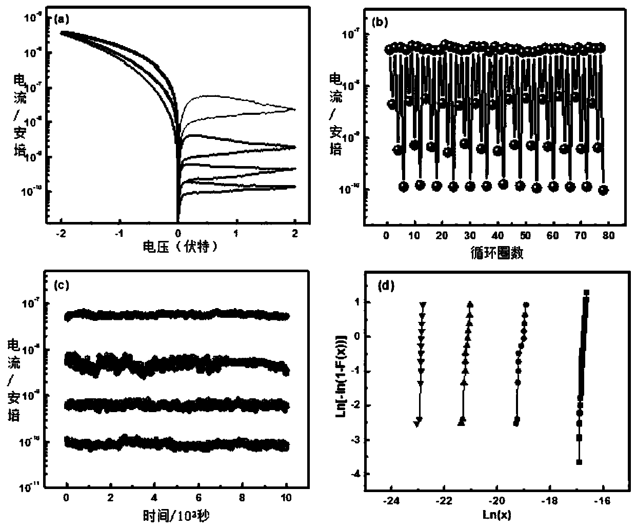
[0056] Such as figure 1 ,Schematic diagram of the multi-state storage performance of the Pt / PFTPA-Fc / ITO structure device in the low conduction state. The method comprises the steps of:

[0057] The initial state of the device Pt / PFTPA-Fc / ITO is in a low conduction state, such as figure 1 As shown in a, when a voltage of 0V→-2V→0V is applied (1st cycle), the current of the device changes slowly. Then apply a voltage of 0V→2V→0V (the second circle), the current decreases with the application of the voltage, and the current at 2V is about 10 -7 A, apply the voltage of 0V→2V→0V again (the third circle), the current decreases with the application of the voltage, and the current at 2V decreases to about 10 -8 A, the 0V→2V→0V voltage scan of the 4th and 5th laps will also produce the same effect as the 2nd and 3rd lap scans, that is, 4 positive-phase 0V→2V→0V voltage scans can produce 4 different current states, and the current switching ratio between different current states is...

Embodiment 2

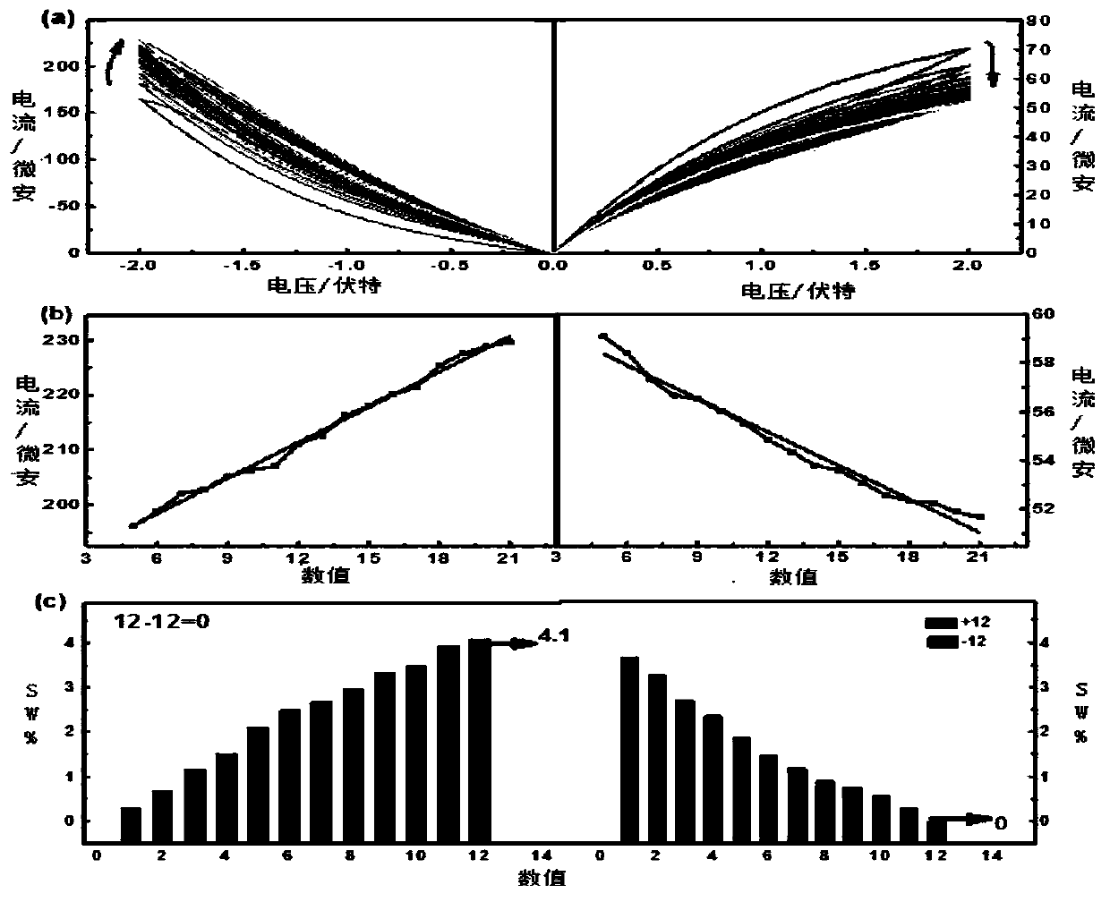
[0059] Such as figure 2 For Pt / PFTPA-Fc / ITO devices in the high current region (>10 -5 A, current-voltage curve of high conduction state). Such as figure 2 As shown in a, under continuous negative voltage (0V→-2V→0V) and positive voltage (0V→2V→0V) sweeps, the current of the device can be continuously regulated. During the negative scanning voltage process of 0V→-2V→0V, the absolute value of the current of the device will increase slowly with the increase of the number of scans, and the absolute value of the current at -2V increases from 165.1μA to 229.5μA; at 0V→2V →During the negative scanning voltage of 0V, the absolute value of the current of the device will slowly decrease with the increase of the number of scans, and the absolute value of the current at 2V decreases from 70.3 μA to 51.7 μA. Such as figure 2 b is the relationship between the absolute value of the current at the voltage of ±2V and the number of scans (the last 17 scans). It can be seen from the figu...

Embodiment 3

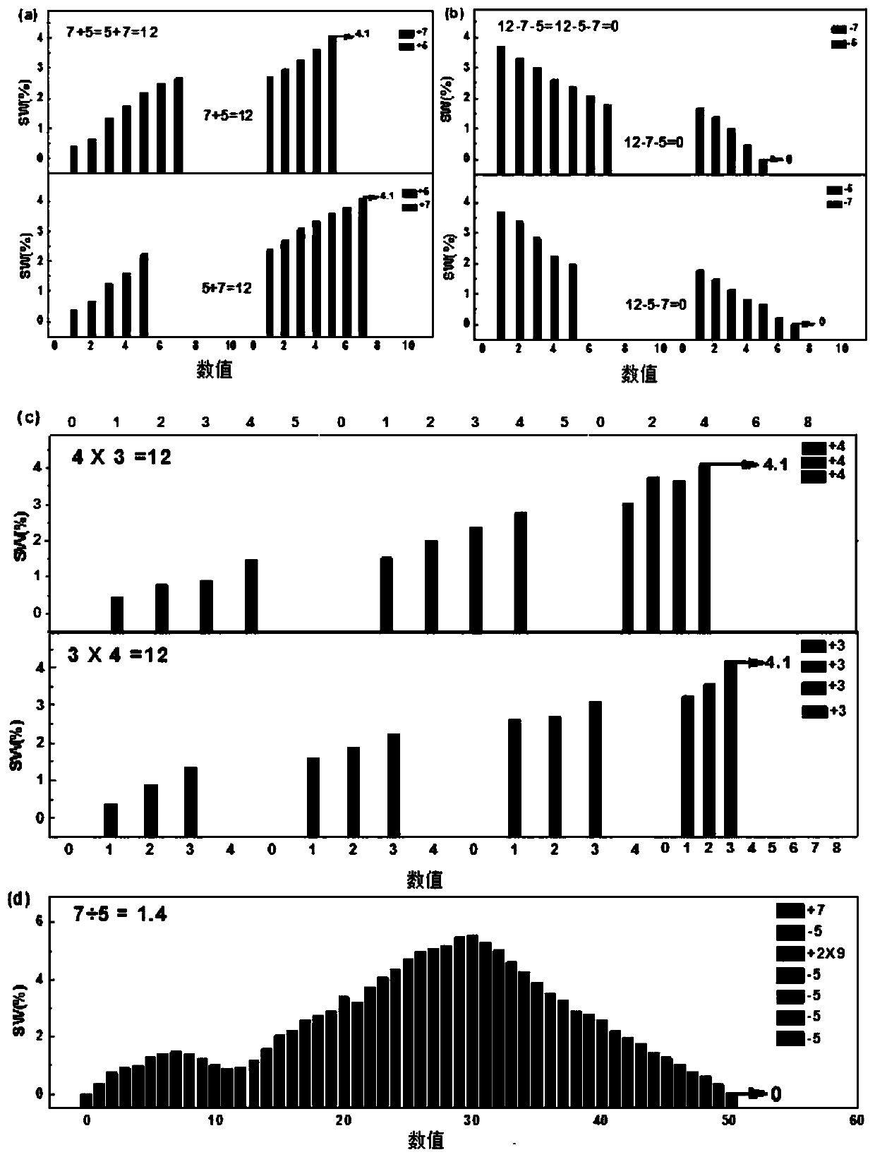
[0062] Such as Figure 4 , this example studies the logic processing of the device in the high conduction state and realizes the 'OR' (or) logic gate, that is, as long as one of the inputs is a logic "1", the output is a logic "1", only when all the inputs When all are logic "0", the output is logic "0". Such as Figure 4 As shown in a, set two conditions: (1) Positive pulse (amplitude of 2V, continuous time of 30ms) as input "0", negative pulse (amplitude of -2V, continuous time of 30ms) as input "1" "; (2) When the device is in the high conduction state, the initial current (with 0.2V as the read voltage) is 10.36μA. If the obtained current at 0.2V is greater than the initial current of 10.36μA, the result is 1, and if the obtained current at 0.2V is less than the initial current of 10.36μA, the result is 0. Figure 4 b shows the output experimental results obtained after different input conditions, from which it can be seen that as long as there is a logic "1" in the inp...


PUM


Abstract

The invention belongs to the field of organic/macromolecular information storage devices, and particularly provides a macromolecular memristor with information storage and data processing capabilitiesat the same time, and a preparation method and an application thereof. The memristor is of a classical sandwich structure; a bottom electrode is Pt; an active layer is a polyfluorene PFTPA-Fc thin film with a side chain containing triphenylamine and ferrocene redox groups; and a top electrode is ITO. By applying different voltages to the memristor, current and voltage curves shows different characteristics: multi-state storage can be realized in a low-conductivity state, and arithmetic and logical operation functions can be realized in a high-conductivity state. In addition, the memristor canachieve free switching between the high-conductivity state and the low-conductivity state. The multi-state storage and operation functions are integrated into the single memristor through macromolecular design and electrical performance regulation, so that a high-performance electronic device is obtained; and the method is an effective means for meeting the ever-increasing data storage and processing requirements at present.

Description

technical field [0001] The invention belongs to the field of organic / polymer information storage devices, in particular to a polymer memristor with both storage and computing functions Background technique [0002] With the rapid development of Internet, mobile network, GPS, weather monitoring, security monitoring, media and other industries, the amount of information has exploded in recent years. As Andreas Wiegand, the former chief scientist of Amazon, said, "Data is the new oil." If the data can be mined and used in time, it will produce huge benefits. In order to realize the mining and application of data, the data must first be stored and processed in a timely manner. Over the past few decades, electronic devices have been developing along Moore's Law, that is, under the condition of constant price, performance doubles every 18-24 months. In order to achieve the goal of doubling performance every 18-24 months, the semiconductor industry usually improves performance by...

Claims


Application Information

Patent Timeline
IPC IPC(8): H01L51/00C08G61/10
CPCC08G61/10C08G2261/124C08G2261/1434C08G2261/146C08G2261/15C08G2261/18C08G2261/3142C08G2261/411C08G2261/72H10K99/00H10K85/10
Inventor 张斌樊菲侯杰陈彧
Owner EAST CHINA UNIV OF SCI & TECH
Why Eureka
Try Eureka