A method for removing silicon nitride in radio frequency ldmos planarization process

A planarization process, silicon nitride technology, applied in the manufacture of electrical components, circuits, semiconductor/solid-state devices, etc., can solve the problems of difficult corrosion, increase the corrosion time, increase the thickness loss of the buffer oxide layer, etc., achieve uniform removal, improve Device performance, buffer oxide loss controllable effect

Active Publication Date: 2020-12-18
NO 55 INST CHINA ELECTRONIC SCI & TECHNOLOGYGROUP CO LTD
View PDF14 Cites 0 Cited by
  • Summary
  • Abstract
  • Description
  • Claims
  • Application Information

AI Technical Summary

Problems solved by technology

Since the corrosion rate of silicon nitride by phosphoric acid decreases with time, the corrosion rate of silicon oxide remains basically the same. Silicon nitride and oxide layers appear alternately at the bird's beak, and the thickness of silicon nitride is thicker, which makes it more difficult to corrode the bird's beak than other positions. Corrosion, simply increasing the corrosion time will increase the loss of buffer oxide thickness

Method used


Image

  • A method for removing silicon nitride in radio frequency ldmos planarization process
  • A method for removing silicon nitride in radio frequency ldmos planarization process
  • A method for removing silicon nitride in radio frequency ldmos planarization process

Examples


Embodiment 1

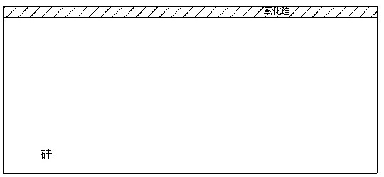
[0049] (1) Oxidative growth of 1000Å first buffer SiO on the surface of the wafer 2 layer;

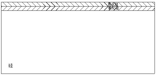
[0050] (2) Deposit 1500Å Si on the surface of the buffer oxide layer by LPCVD 3 N 4 ;

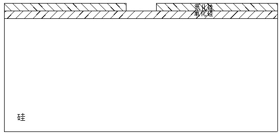
[0051] (3) Photolithography, dry etching surface Si 3 N 4 , SiO 2 , terminated in buffered SiO 2 layer; remove the photoresist to form an oxide window;

[0052] (4) HF: H 2 O=1:10 concentration HF corrosion buffer SiO 2 layer for 3 minutes until the surface is hydrophobic;

[0053] (5) Perform the first wet oxygen oxidation with a thickness of 9800Å;

[0054] (6) Buffered hydrofluoric acid corrodes the first wet oxygen SiO 2 layer, time 10 minutes, surface hydrophobic;

[0055] (7) Oxidative growth of the second buffer SiO 2 Layer thickness is 800 Å;

[0056] (8) In buffered SiO 2 LPCVD deposited Si on the surface of the layer 3 N 4 , with a thickness of 800 Å;

[0057] (9) Dry etching of Si deposited by LPCVD 3 N 4 , Si at the oxidation window 3 N 4 Etched clean, active Si 3 ...

Embodiment 2

[0062] (1) Oxidative growth of 1000Å first buffer SiO on the surface of the wafer 2 layer;

[0063] (2) Deposit 1510Å Si on the surface of buffer oxide layer 1 by LPCVD 3 N 4 ;

[0064] (3) Photolithography, dry etching surface Si 3 N 4 , SiO 2 , terminated in buffered SiO 2 layer; remove the photoresist to form an oxide window;

[0065] (4) HF: H 2 O=1:10 concentration HF corrosion buffer SiO 2 layer for 3 minutes until the surface is hydrophobic;

[0066] (5) Perform the first wet oxygen oxidation with a thickness of 9885Å;

[0067] (6) Buffered hydrofluoric acid corrodes the first wet oxygen SiO 2 layer, time 10 minutes, surface hydrophobic;

[0068] (7) Oxidative growth of the second buffer SiO 2 Layer thickness is 500 Å;

[0069] (8) In buffered SiO 2 LPCVD deposited Si on the surface of the layer 3 N 4 , with a thickness of 800 Å;

[0070] (9) Dry etching of Si deposited by LPCVD 3 N 4 , Si at the oxidation window 3 N 4 Etched clean, active Si 3 N ...


PUM

PropertyMeasurementUnit
thicknessaaaaaaaaaa
thicknessaaaaaaaaaa
thicknessaaaaaaaaaa

Abstract

The invention relates to a method for removing silicon nitride in a radio frequency LDMOS planarization process, which is characterized in that, for the masking medium after two times of wet oxygen planarization, the etching rate at the edge of the pattern is higher than that in the middle, and the nitrogen at the edge of the bird's beak The silicon nitride thickness is greater than the middle position of the pattern, and the silicon nitride is removed by two phosphoric acid etching methods. Advantages: 1) It solves the problem of uneven removal of silicon nitride after the planarization process in the production of LDMOS devices, resulting in damage to the active area and the problem of more buffer oxide layer loss after etching and removing silicon nitride. 2) Two new phosphoric acid etching processes are adopted to ensure the uniform removal of silicon nitride in the active area, and at the same time ensure that the loss of the buffer oxide layer after silicon nitride removal is controllable, the LOCOS planarization process is easier to implement, and the device performance is improved.

Description

technical field [0001] The invention relates to a method for removing silicon nitride in a radio frequency LDMOS planarization process, and belongs to the technical field of semiconductor microelectronic design and manufacture. Background technique [0002] In the field of microwave technology, radio frequency LDMOS devices are more and more widely used in communication base stations, broadcast television and modern radar systems. In order to continuously improve the frequency performance of LDMOS, the feature size of the LDMOS gate is continuously reduced, from the initial micron level to the current sub-micron level, and device production requires higher and higher surface flatness. One of the important methods to realize device isolation is local oxidation on silicon (LOCOS). Among them, the planarization effect of the two oxidations is better. In the process, the insulation medium is filled outside the active area, and the oxide medium is used to increase the thickness...

Claims


Application Information

Patent Timeline
Patent Type & Authority Patents(China)
IPC IPC(8): H01L21/311
CPCH01L21/31111
Inventor 吕勇赵杨杨刘洪军王佃利严德圣庸安明梅海
Owner NO 55 INST CHINA ELECTRONIC SCI & TECHNOLOGYGROUP CO LTD
Why Eureka
Try Eureka