
Manufacturing process of diode chip with lateral electrode and shallow trench

A manufacturing process and diode technology, applied in semiconductor/solid-state device manufacturing, circuits, electrical components, etc., can solve problems such as affecting the reliability and service life of devices, increasing the complexity of the circuit connection process, and being unfavorable for product miniaturization. Wide range of process applications, improved heat dissipation performance, and reduced material costs

Pending Publication Date: 2019-07-26
SUZHOU GOODARK ELECTRONICS CO LTD
View PDF0 Cites 1 Cited by
  • Summary
  • Abstract
  • Description
  • Claims
  • Application Information

AI Technical Summary

Problems solved by technology

[0004] 1. Since the PN junction is formed by the process of diffusion on both sides of the chip, it is not conducive to the miniaturization of the product;
[0005] 2. There are electrodes and lead frames on both sides of the chip, which further increases the thickness and the complexity of the circuit connection process, and in the subsequent packaging process, the chip cannot be in direct contact with the outer heat sink, and the heat dissipation effect will also be affected;
The power consumption of this part of diode heating not only affects the reliability and service life of the device due to continuous heating, but also consumes a lot of unnecessary energy, which is incompatible with the current environmental protection requirements for green energy saving

Method used


Image

  • Manufacturing process of diode chip with lateral electrode and shallow trench
  • Manufacturing process of diode chip with lateral electrode and shallow trench
  • Manufacturing process of diode chip with lateral electrode and shallow trench

Examples


Embodiment

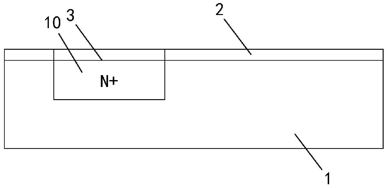
[0074] Example: see attached Figure 1~11 As shown, a manufacturing process of a diode chip with electrodes on the same side of a shallow trench; first, a silicon substrate 1 is selected, and the silicon substrate 1 can be selected from an N-type crystal orientation or a P-type crystal orientation, This embodiment takes the N-type crystal orientation as an example for illustration, and then proceeds according to the following steps:

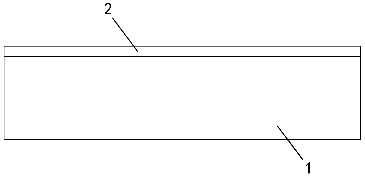
[0075] first step, such as figure 1 As shown, a layer of first silicon dioxide thin film layer 2 is formed on the upper surface of the silicon wafer substrate 1; the process conditions for the formation of the first silicon dioxide thin film layer 2 are: 1150 ± 0.5 ° C furnace tube, first through 30±5 minutes of oxygen (O 2 ) atmosphere, and then after 480±10 minutes of water vapor (H 2 O) atmosphere, and finally oxygen (O 2 )atmosphere.

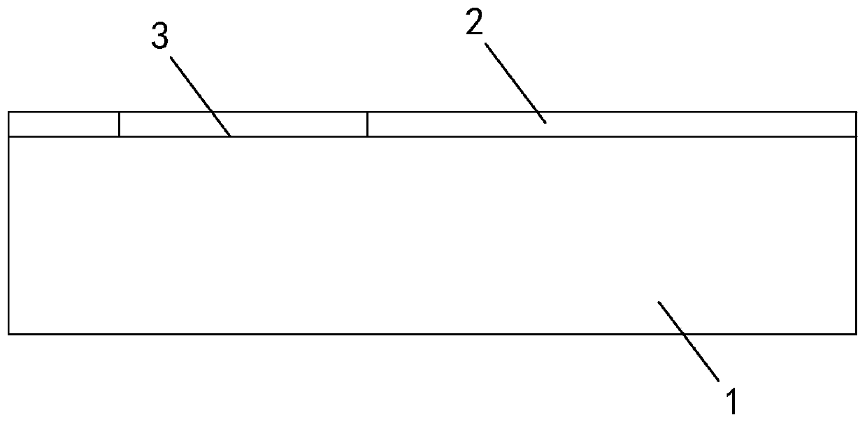
[0076] The second step, such as figure 2 As shown, the peripheral area of ​​the first silicon diox...


PUM

PropertyMeasurementUnit
Thicknessaaaaaaaaaa

Abstract

A manufacturing process of a diode chip with a lateral electrode and a shallow trench. The steps include: a first silicon dioxide film layer is formed on the surface of a silicon substrate; a first region of the first silicon dioxide film layer is etched and removed; the first region is subjected to a first doping to form an N+ region; the first silicon dioxide film layer is removed and a second silicon dioxide film layer is formed after cleaning; a second region of the second silicon dioxide film layer is etched and removed, which is spaced apart from the first region; the second region is subjected to a second doping to form a P+ region; a trench is prepared in an edge region of the N+ region or the P+ region; the second silicon dioxide film layer is removed; a polysilicon passivation composite film layer is formed after cleaning; a glass passivation layer is formed in the trench; the polysilicon passivation composite film layer on the surface of the first and second regions is removed and the N+ region and P+ region are exposed; and a metal layer is deposited on the surface of the N+ region and P+ region to form a metal electrode. The electrode of the invention is at the same side; the volume is small; the cost is low and the electrical performance is excellent.

Description

technical field [0001] The invention relates to a diode manufacturing process, in particular to a manufacturing process of a diode chip on the same side as an electrode in a shallow groove. Background technique [0002] Diodes are widely used in various circuits. It can be said that there are diodes wherever there is a circuit. It uses its unidirectional conduction characteristics to convert alternating current into direct current, so that the terminal parts of the circuit can obtain stable direct current input. The current manufacturing method of rectifier diodes is based on the N-type <111> crystalline silicon wafer as the basic material, performing a boron doping on the upper surface of the silicon wafer to form a flat P region, and then performing a phosphorus diffusion on the lower surface to form a flat P region. The flat N region is then processed by photolithography, metallization, alloying and other processes, and finally the PN structure and electrode metal o...

Claims


Application Information

Patent Timeline
IPC IPC(8): H01L29/861H01L29/06H01L21/329H01L23/367H01L23/373H01L23/31H01L21/228H01L23/29
CPCH01L29/8611H01L29/0603H01L29/0688H01L29/66128H01L23/367H01L23/3731H01L23/3121H01L21/228H01L23/291H01L23/298H01L23/3178
Inventor 吴念博
Owner SUZHOU GOODARK ELECTRONICS CO LTD
Learn More