Supercharge Your Innovation With Domain-Expert AI Agents!

Stripping method of SiC-based GaN epitaxial wafer

A technology of epitaxial wafers and oxygen ions, which is applied in the field of semiconductors, can solve the problems of low stacking fault formation energy, SiC substrate waste, and increased difficulty, and achieve the effects of easy subsequent stripping, increased utilization rate, and simple process

Inactive Publication Date: 2019-08-02
XIAMEN SANAN INTEGRATED CIRCUIT
View PDF7 Cites 4 Cited by
  • Summary
  • Abstract
  • Description
  • Claims
  • Application Information

AI Technical Summary

Problems solved by technology

As the only stable compound of C and Si, SiC has a lattice structure composed of two densely arranged sublattices, and each Si (or C) atom and surrounding C (or Si) atoms pass through the oriented strong tetrahedral SP 3 Bonding, although the tetrahedral bond of SiC is very strong, but the stacking fault formation energy is very low, this characteristic determines the polytype phenomenon of SiC, and the stacking order of the C / Si double atomic layer of each polytype is different , leading to the complex growth process of SiC single crystal, and many process parameters affect the final crystal quality, which leads to very expensive SiC substrates and high chip development costs
[0004] Due to the limited warpage and total thickness variation of SiC wafer processing, and the influence of temperature and stress during the epitaxial growth of SiC-based GaN, the SiC substrate needs to be at least 500um, but in practical applications, SiC-based GaN devices are not thick enough in practical applications 120um, in the traditional process, the excess SiC substrate is removed by grinding, resulting in waste of 400um SiC substrate
However, this method has the following disadvantages: H 2 Si-H bonds are formed after implantation, and Si-H bonds will be broken during the growth of GAN (atmosphere above 900°C), and the SiC lattice will be easily repaired, and subsequent high-temperature tempering and laser lift-off will increase the difficulty

Method used


Image

  • Stripping method of SiC-based GaN epitaxial wafer
  • Stripping method of SiC-based GaN epitaxial wafer
  • Stripping method of SiC-based GaN epitaxial wafer

Examples


Embodiment Construction

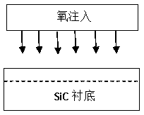
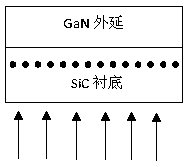
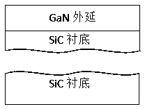
[0028] The present invention will be further described in detail below in conjunction with the accompanying drawings and specific embodiments. Disclosed in the present invention is a method for stripping off a SiC-based GaN epitaxial wafer, such as figure 1 , figure 2 and image 3 As shown, it specifically includes the following steps: Step S1: By implanting oxygen ions, an oxygen layer and a SiO layer are formed under the surface of the SiC substrate. 2 , at the same time, react to form a bubble layer; step S2: generate GaN epitaxy on the surface layer of the substrate; step S3: perform laser cutting along the bubble layer to obtain SiC-based GaN epitaxial wafers. The remaining SiC substrates can be recycled, thereby increasing the utilization rate of SiC substrates.

[0029] Further, in step S1, before implanting oxygen ions, a silicon nitride dielectric layer is deposited on the SiC substrate to protect the interface of the SiC substrate. The thickness of the dielectri...


PUM

PropertyMeasurementUnit
thicknessaaaaaaaaaa
thicknessaaaaaaaaaa

Abstract

The invention discloses a stripping method of a SiC-based GaN epitaxial wafer. The stripping method comprises the following specific steps: S1, forming an oxygen layer and SiO2 under the surface layerof a SiC substrate by implanting oxygen ions, and reacting to form a bubble layer; S2, producing GaNepitaxy on the surface layer of the SiC substrate; S3, performing laser cutting along the bubble layer to obtain the SiC-based GaN epitaxial wafer. According to the stripping method, the SiC substrate can be stripped off quickly and efficiently, so that the SiC substrate is recycled and the usage rate of the SiC substrate is increased.

Description

technical field [0001] The invention relates to the technical field of semiconductors, in particular to a method for peeling off SiC-based GaN epitaxial wafers. Background technique [0002] SiC materials have good physical and chemical properties, such as stable chemical properties, small thermal expansion coefficient, corrosion resistance, wear resistance, high strength, high hardness, etc., so they have broad applications in the fields of mechanical electronics, composite materials, and aerospace. Application prospects. Especially with the rapid development of modernization of weapons and equipment and the continuous development of various advanced technologies, the demand for high-performance electronic devices working in harsh environments such as high temperature resistance and radiation resistance is becoming increasingly urgent. A number of limitations have emerged. Therefore, the third generation of semiconductor materials represented by wide bandgap semiconductor...

Claims


Application Information

Patent Timeline
Patent Type & Authority Applications(China)
IPC IPC(8): C30B25/18C30B29/40
CPCC30B25/183C30B25/186C30B29/406
Inventor 蔡仙清蔡文必刘胜厚邹鹏辉许若华卢益锋杨健
Owner XIAMEN SANAN INTEGRATED CIRCUIT
Features
  • R&D
  • Intellectual Property
  • Life Sciences
  • Materials
  • Tech Scout
  • Unparalleled Data Quality
  • Higher Quality Content
  • 60% Fewer Hallucinations
Learn More