A method of splicing and growing large-scale single crystal diamond epitaxial wafers

A single crystal diamond and growth method technology, applied in the directions of single crystal growth, single crystal growth, crystal growth, etc., can solve the difficulty of preparing single crystal diamond wafers for diamond semiconductor devices, the technical complexity, and the preparation of large-size single crystal diamond materials. The problem has not been well solved, etc., to achieve the effect of low cracking and breaking probability, increasing size limit, and small residual stress

Active Publication Date: 2020-10-02
ZHENGZHOU RES INST FOR ABRASIVES & GRINDING CO LTD
View PDF8 Cites 1 Cited by
  • Summary
  • Abstract
  • Description
  • Claims
  • Application Information

AI Technical Summary

Problems solved by technology

The current technology has generally achieved 8-10 mm high quality (diamond 1332 cm -1 Raman peak width at half maximum is less than 2.6 cm -1 ) epitaxial growth of single crystal diamond wafers, but due to the lack of larger seed crystals as substrates for single crystal diamond epitaxial growth, the preparation of inch-scale (>1 inch) single crystal diamond wafers for the development of diamond semiconductor devices still faces challenges focus on difficulties
[0004] At present, in the preparation process of large-sized single-crystal diamond materials, the method of splicing and growing smaller-sized single-crystal diamonds according to a consistent crystal orientation is usually used to obtain larger-sized single-crystal diamonds, as reported by Yamada in their research. The splicing growth method of 1-inch and 2-inch single crystal diamond [1, 2] has been proved, and the feasibility of obtaining splicing growth of large-size single-crystal diamond materials has been confirmed. The preparation of materials has not yet been well resolved

Method used


Image

  • A method of splicing and growing large-scale single crystal diamond epitaxial wafers
  • A method of splicing and growing large-scale single crystal diamond epitaxial wafers
  • A method of splicing and growing large-scale single crystal diamond epitaxial wafers

Examples


Embodiment Construction

[0029] In order to make the technical purpose, technical solution and beneficial effect of the present invention clearer, the technical solution of the present invention will be further described below in conjunction with the drawings and specific embodiments.

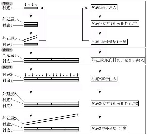
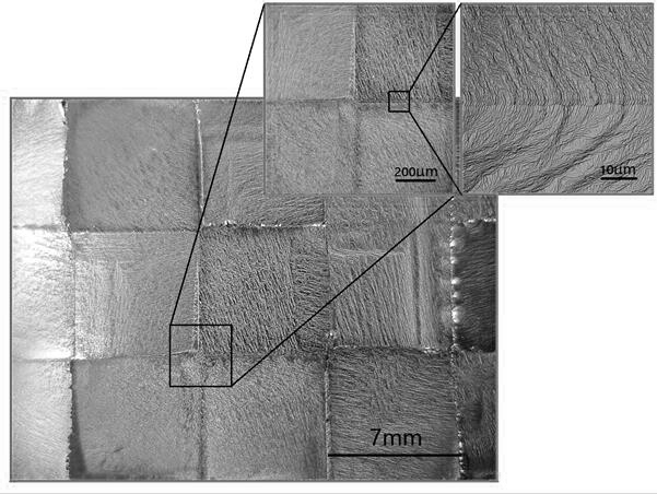
[0030] The specific preparation process of the present invention is as figure 1 As shown, firstly, the chemical vapor deposition method is selected to synthesize macro-defect-free, and the dislocation density is lower than 5000 / cm 2 The single crystal diamond is used as the substrate 1, the substrate 1 is cut and polished, the direction error between the cutting surface and the (100) crystal plane does not exceed ±1°, and the cutting size is 7×7mm 2 , Flaky square crystals with a thickness of 0.5mm. Grinding and polishing the cut substrate 1, the roughness of the upper and lower main surfaces of the crystal after polishing is not more than 5nm, and the roughness of the four sides is not more than 100nm.

[0031] Impl...


PUM

PropertyMeasurementUnit
sizeaaaaaaaaaa
surface roughnessaaaaaaaaaa

Abstract

The invention provides a mosaic growth method of a large-size single-crystal diamond epitaxial wafer to overcome defects in mosaic preparation of large-size single-crystal diamond. Firstly, by use ofion injection and separation technologies, multiple single-crystal diamond epitaxial wafers with strictly consistent crystal orientation are obtained after chemical vapor deposition, then, the epitaxial wafers are arranged along consistent crystal orientation and bonded on a substrate, then, flattening processing and ion injection are performed, and finally, the large-size single-crystal diamond epitaxial wafer is obtained after chemical vapor deposition and separation. The single-crystal diamond epitaxial wafer of 1-6 inches can be obtained with the method, and the quality of crystals epitaxially growing at mosaic interfaces does not obviously deteriorate.

Description

technical field [0001] The invention belongs to the technical field of large-size single crystal diamond preparation, and in particular relates to a method for splicing and growing large-size single crystal diamond epitaxial wafers. Background technique [0002] As the basic material for the development of electricity, electronics and information technology, the performance of the first-generation semiconductor materials represented by Si has gradually approached the theoretical limit in terms of device operating voltage, power consumption, and device response speed. Traditional Si semiconductor devices are Faced with gradual replacement. The application requirements in the fields of high power, low loss, high temperature, and high frequency have prompted the emergence of a new batch of wide bandgap semiconductor materials such as SiC, GaN, and diamond. Compared with Si semiconductor materials, the band gap, breakdown electric field, carrier mobility, and thermal conductivi...

Claims


Application Information

Patent Timeline
Patent Type & Authority Patents(China)
IPC IPC(8): C30B25/22C30B29/04
CPCC30B25/22C30B29/04
Inventor 闫宁赵延军范波徐帅
Owner ZHENGZHOU RES INST FOR ABRASIVES & GRINDING CO LTD
Why Eureka
Try Eureka