Slot antenna coupled superconducting transition edge polarization detector array and preparation technology thereof
A detector array and slot antenna technology, applied in the field of superconducting detectors, can solve the problems of bracket damage, unobservation, pollution, etc., and achieve the effects of avoiding bracket damage, rational wiring, and improving sensitivity
- Summary
- Abstract
- Description
- Claims
- Application Information
AI Technical Summary
Problems solved by technology
Method used
Image
Examples
Embodiment 1
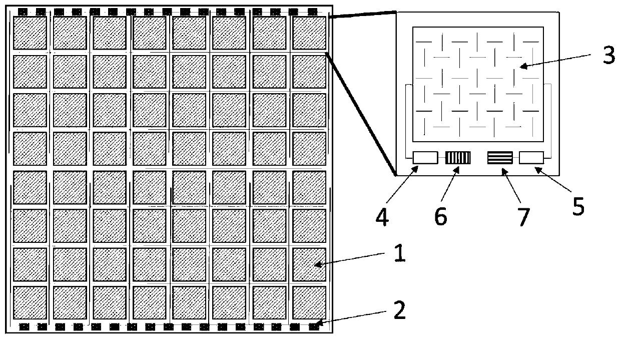
[0043] Such as figure 1 As shown, a slot antenna coupled superconducting transition edge polarization detector array has 64 (8×8 array) pixel units 1, and 512 wire bonding points 2 are distributed at the upper and lower ends of the entire array. Each pixel unit 1 includes a slot antenna array 3, and the slot antenna array 3 is connected to a band-pass filter-4 and a superconducting transition edge sensor-6 acting on microwave signals in the vertical direction and a band-pass filter acting on microwave signals in the horizontal direction 25 and superconducting transition edge sensors 27.
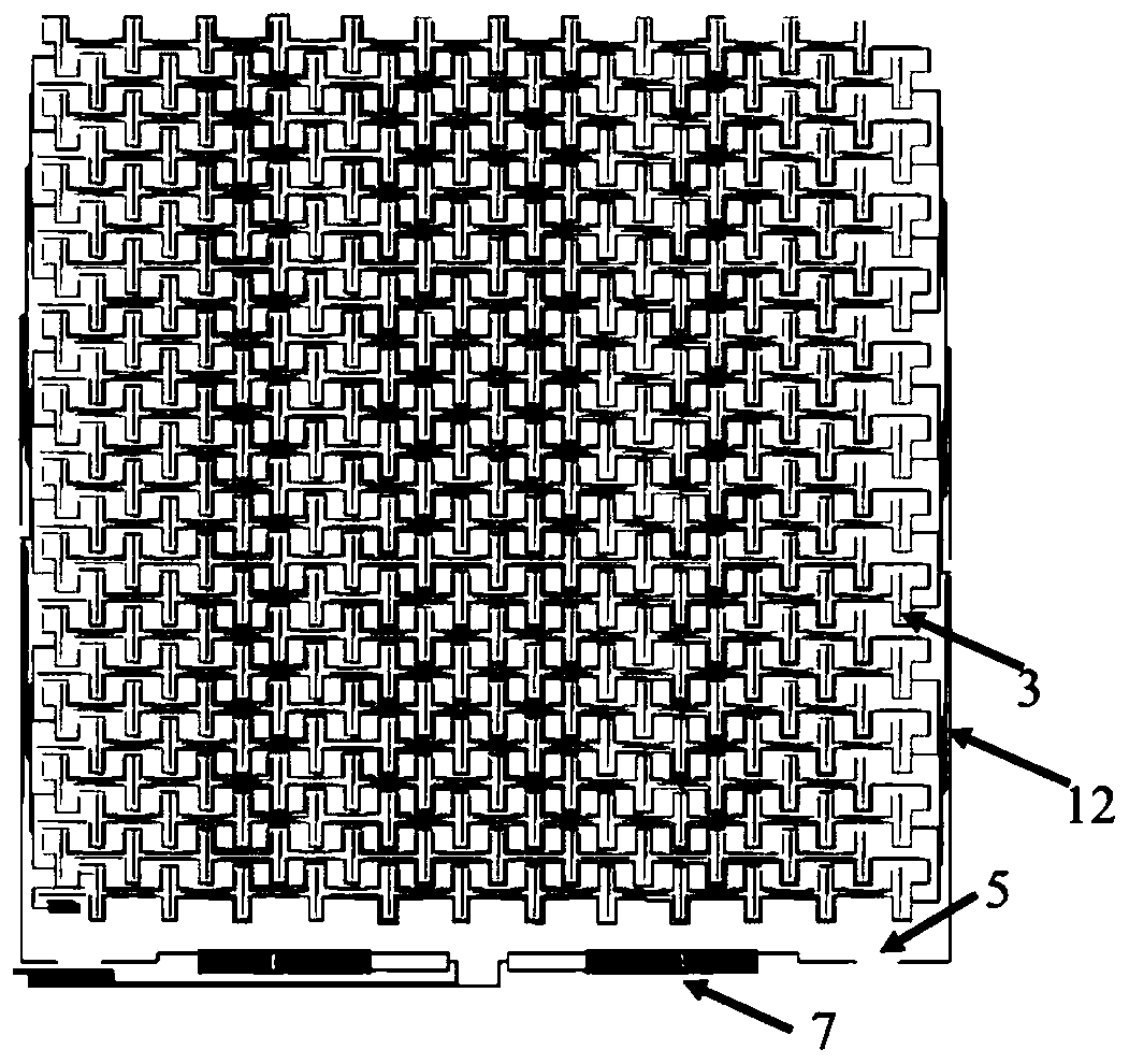
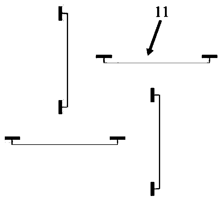
[0044] Such as figure 2 and image 3 As shown, each slot antenna array 3 is made up of 144 (12×12 arrays) slot antenna array units and a microstrip feed network 12, and each of the slot antenna array units is composed of four slot antennas 11 and each The slot antenna 11 is composed of symmetrical feed lines at both ends, wherein, among the four slot antennas 11, two are horizontal slots ...
Embodiment 2
[0064] Its structure is consistent with embodiment 1, and the superconducting metal film A13 material is Mo; The superconducting metal film B is Ti, and the preparation technology of this slot antenna coupling type superconducting conversion edge polarization detector array comprises the following steps:
[0065] Step 1. Use a 4-inch high-resistance double-sided polished silicon wafer, and use thermal oxidation to grow 800nm thick SiO on both sides of the silicon wafer. 2 thin film, then SiO on the front side 2 A low-stress silicon nitride film with a thickness of 3.0 μm was grown on the film using low-pressure chemical vapor deposition technology.
[0066] Step 2. On the front side of the sample obtained in step 1, a 200nm thick Mo film is prepared by magnetron sputtering, and then the first photolithography is performed, and the Mo pattern of the superconducting film is obtained by etching.
[0067] Step 3. On the front side of the sample obtained in step 2, grow SiO wit...
Embodiment 3
[0079] Its structure is consistent with embodiment 1, and superconducting metal film A13 material is AlMn alloy; Superconducting metal film B is Ti, and the preparation technology of this slot antenna coupled type superconducting conversion edge polarization detector array comprises the following steps:
[0080] Step 1. Use a 4-inch high-resistance double-sided polished silicon wafer, and use thermal oxidation to grow 300nm thick SiO on both sides of the silicon wafer. 2 thin film, then SiO on the front side 2 A low-stress silicon nitride film with a thickness of 1.5 μm is grown on the film using low-pressure chemical vapor deposition technology.
[0081] Step 2. On the front side of the sample obtained in step 1, a 150nm thick AlMn film is prepared by magnetron sputtering, and then photolithography is performed for the first time, and a superconducting thin film AlMn pattern is obtained by etching.
[0082] Step 3. On the front side of the sample obtained in step 2, grow Si...
PUM
| Property | Measurement | Unit |
|---|---|---|
| Thickness | aaaaa | aaaaa |
| Thickness | aaaaa | aaaaa |
| Thickness | aaaaa | aaaaa |
Abstract
Description
Claims
Application Information


