Method for preparing magnetic tunnel junction unit array

A technology of magnetic tunnel junction and cell array, which is applied in the fields of magnetic field-controlled resistors, electromagnetic device manufacturing/processing, digital memory information, etc., and can solve the problems of unfavorable magnetic tunnel junction magnetism, electricity, and yield.

Active Publication Date: 2019-08-09
SHANGHAI CIYU INFORMATION TECH
View PDF9 Cites 7 Cited by
  • Summary
  • Abstract
  • Description
  • Claims
  • Application Information

AI Technical Summary

Problems solved by technology

[0004] However, when performing chemical mechanical planarization on patterned CMOS via holes, due to the existence of butterfly defects, the surface flatness will not meet the requirements for making magnetic tunnel junctions (MTJ), which will It is very detrimental to the improvement of the magnetic properties, electricity and yield of the magnetic tunnel junction (MTJ). Patent US2018/0358070A1 discloses a method for fabricating a magnetic tunnel junction (MTJ). Immediately after fabrication, a layer of bottom electrode (Bottom Electrode, BE) is deposited, and a chemical mechanical polishing (CMP) process is selected to planarize the bottom

Method used


Image

  • Method for preparing magnetic tunnel junction unit array
  • Method for preparing magnetic tunnel junction unit array
  • Method for preparing magnetic tunnel junction unit array

Examples


Embodiment Construction

[0024] The following will clearly and completely describe the technical solutions in the embodiments of the present invention with reference to the accompanying drawings in the embodiments of the present invention. Obviously, the described embodiments are only some, not all, embodiments of the present invention.

[0025] see Figure 1 to Figure 10 , the present invention provides a technical solution: a method for preparing a magnetic tunnel junction unit array, comprising:

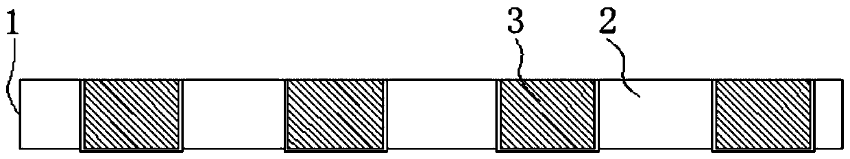
[0026] Step 1: Provide a surface-polished CMOS substrate 1 with metal wiring Mx (x≥1), wherein the material of metal wiring Mx (x≥1)3 is Cu, such as figure 1 shown.

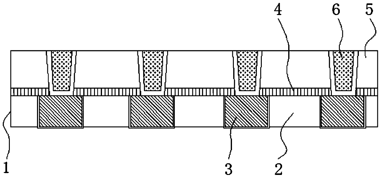
[0027] Step 2: On the surface-polished CMOS substrate 1 with metal wiring Mx (x≥1), make the bottom electrode through hole (BEV) 6, such as figure 2 shown.

[0028] Wherein, the BEV etching barrier layer 4 is SiN, SiN, SiC or SiCN, etc., and the BEV interlayer dielectric 5 is SiO 2 , SiON or low dielectric constant (Low-K) dielectric, ...


PUM

PropertyMeasurementUnit
Thicknessaaaaaaaaaa
Thicknessaaaaaaaaaa
Thicknessaaaaaaaaaa

Abstract

The invention discloses a method for preparing a magnetic tunnel junction unit array. The method concretely comprises the steps of: providing a CMOS substrate with a metal connection line Mx (x is notless than 1) with a polished surface; on the CMOS substrate with the metal connection line Mx with the polished surface, manufacturing a BEV (Bottom Electrode Via); manufacturing a bottom electrode contact/bottom electrode on the BEV; depositing a magnetic tunnel junction multilayer film and a top electrode on the flattened bottom electrode, graphically defining a magnetic tunnel junction pattern, etching the top electrode, the magnetic tunnel junction and the bottom electrode metal, and finally depositing an insulating covering layer around the etched magnetic tunnel junction. The method forpreparing the magnetic tunnel junction unit array manufactures a W BEV, a non-Cu bottom electrode contact/bottom electrode, a magnetic tunnel junction and a top electrode on a CMOS metal connecting line with the polished surface, and allows BEV (Bottom Electrode Via), BEC (Bottom Electrode Contact), BE (Bottom Electrode), MTJ (Magnetic Tunnel Junction) and TE (Top Electrode) to be sequentially and upwards overlapped and aligned.

Description

technical field [0001] The invention relates to the technical field of magnetic random access memory (Magnetic Random Access Memory, MRAM), in particular to a method for preparing a magnetic tunnel junction cell array. Background technique [0002] In recent years, MRAM using Magnetic Tunnel Junction (MTJ) is considered to be the future solid-state non-volatile memory, which has the characteristics of high-speed reading and writing, large capacity and low energy consumption. Ferromagnetic MTJ is usually Sandwich structure, in which there is a magnetic memory layer, which can change the magnetization direction to record different data; an insulating tunnel barrier layer in the middle; a magnetic reference layer, which is located on the other side of the tunnel barrier layer, and its magnetization direction remains unchanged . [0003] In order to record information in this magnetoresistive element, it is recommended to use a writing method based on spin-momentum transfer or ...

Claims


Application Information

Patent Timeline
IPC IPC(8): H01L43/12H01L43/08G11C11/16
CPCG11C11/161H10N50/10H10N50/01
Inventor 张云森郭一民肖荣福陈峻
Owner SHANGHAI CIYU INFORMATION TECH
Why Eureka
Try Eureka