
Preparation method of CuFeO2 semiconductor

A semiconductor, cuso4-technology, applied in the direction of electrode, electrolytic inorganic material coating, electrolytic process, etc., can solve the problems that affect the stability of semiconductors, light corrosion, reduce water decomposition efficiency, etc., achieve excellent light stability and reduce light corrosion , The effect of Faraday efficiency improvement

Inactive Publication Date: 2019-08-13
FOSHAN UNIVERSITY
View PDF9 Cites 1 Cited by
  • Summary
  • Abstract
  • Description
  • Claims
  • Application Information

AI Technical Summary

Problems solved by technology

Semiconductor materials with an energy band gap of 1.7-2.2eV are ideal photoelectrodes for photoelectrolysis of water, such as Cu 2 O, but Cu 2 O In the process of using solar energy to decompose water to produce hydrogen, photocorrosion also occurs, which seriously affects the stability of semiconductors and reduces the efficiency of water decomposition

Method used

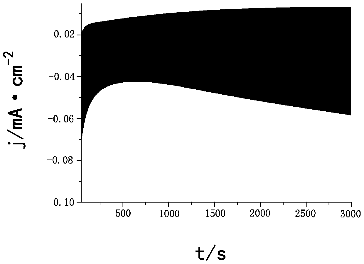
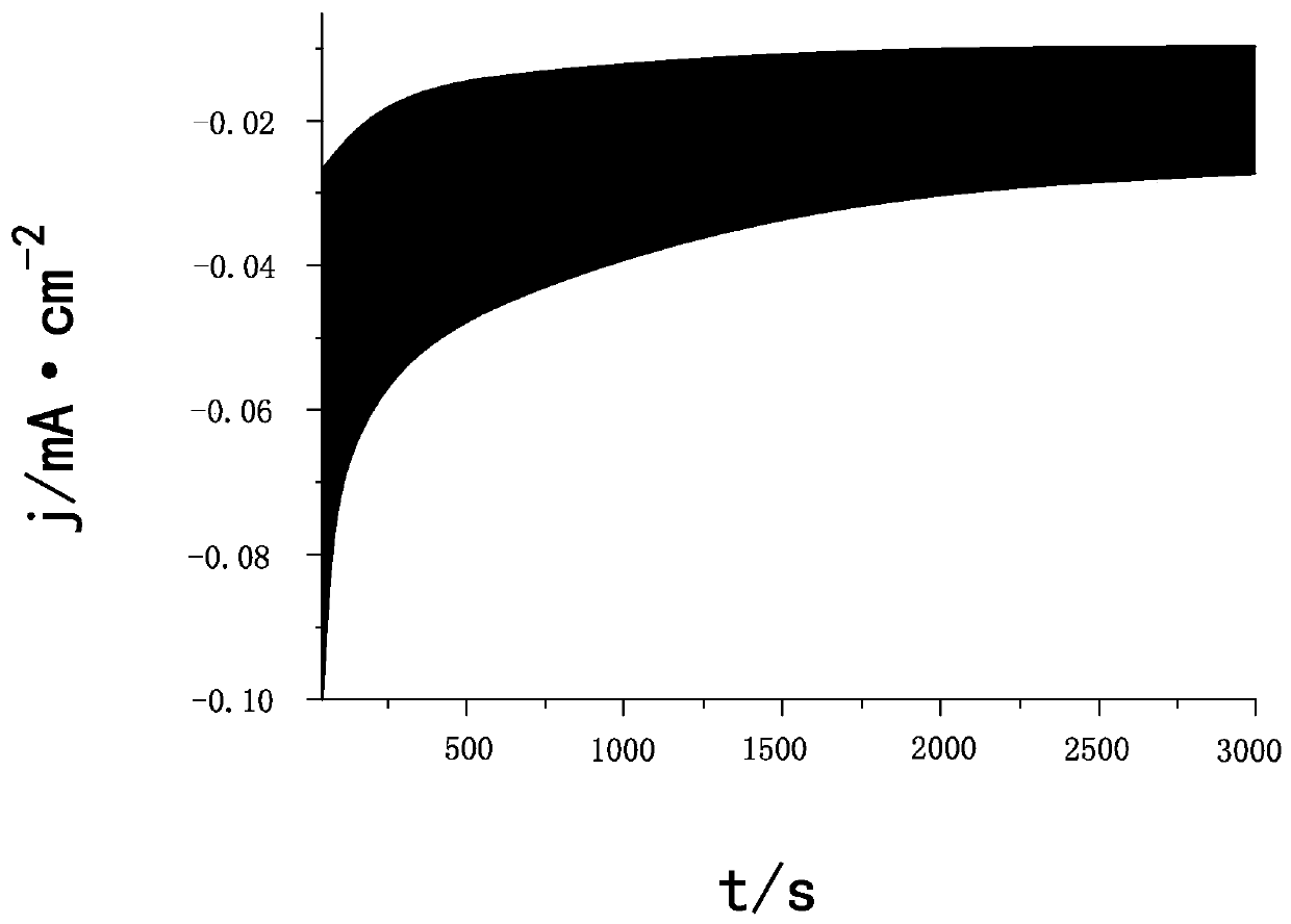
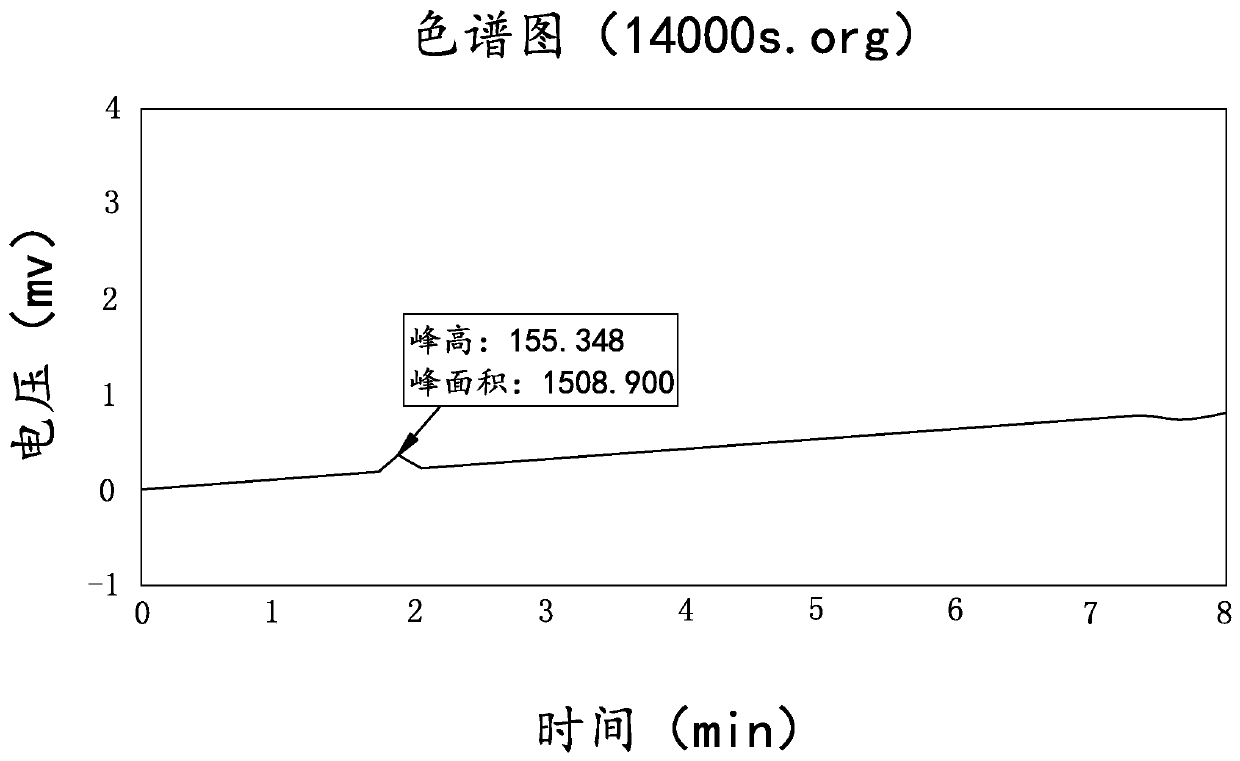

Image

  • Preparation method of CuFeO2 semiconductor
  • Preparation method of CuFeO2 semiconductor
  • Preparation method of CuFeO2 semiconductor

Examples


Embodiment 1

[0024] a CuFeO 2 A method for preparing a semiconductor, comprising the steps of:

[0025] (1) Add CuSO to lactic acid solution 4 solution, after mixing uniformly to obtain CuSO 4 - Lactic acid mixed solution, the resulting CuSO 4 -The concentration of lactic acid in the lactic acid mixed solution is 0.25mol / L, CuSO 4 The concentration is 0.4mol / L;

[0026] (2) CuSO prepared in step (1) 4 -Add FeCl to lactic acid mixed solution 3 , the added FeCl 3 The concentration is 0.05mol / L, and magnetic stirring is used to make FeCl 3 dissolved and mixed with CuSO 4 - Lactic acid mixed solution is mixed evenly to prepare CuFeO 2 Electrodeposition solution;

[0027] (3) CuFeO prepared in step (2) 2 Add alkaline solution to the electrodeposition solution, the alkaline solution used is NaOH solution, adjust CuFeO 2 The pH value of the electrodeposition solution is 7.0;

[0028] (4) ITO conductive glass is put into acetone, ethanol and ultrapure water successively to clean;

[...

Embodiment 2

[0031] a CuFeO 2 A method for preparing a semiconductor, comprising the steps of:

[0032] (1) Add CuSO to lactic acid solution 4 solution, after mixing uniformly to obtain CuSO 4 - Lactic acid mixed solution, the resulting CuSO 4 -The concentration of lactic acid in the lactic acid mixed solution is 0.35mol / L, CuSO 4 The concentration is 0.6mol / L;

[0033] (2) CuSO prepared in step (1) 4 -Add FeCl to lactic acid mixed solution 3 , the added FeCl 3 The concentration is 0.5mol / L, and magnetic stirring is used to make FeCl 3 dissolved and mixed with CuSO 4 - Lactic acid mixed solution is mixed evenly to prepare CuFeO 2 Electrodeposition solution;

[0034] (3) CuFeO prepared in step (2) 2 Add alkaline solution to the electrodeposition solution, the alkaline solution used is NaOH solution, adjust CuFeO 2 The pH value of the electrodeposition solution is 9.5;

[0035] (4) ITO conductive glass is put into acetone, ethanol and ultrapure water successively to clean;

[0...


PUM


Abstract

The invention provides a preparation method of a CuFeO2 semiconductor. According to the technical scheme, iron ions are doped in traditional Cu2O, the pH value of a CuFeO2 electrodeposition solution is adjusted, and CuFeO2 is deposited on ITO conductive glass to prepare the CuFeO2 semiconductor. The prepared CuFeO2 semiconductor is regular in shape, uniform in size and uniform and flat in thickness. Compared with a Cu2O semiconductor, the Faradaic efficiency of CuFeO2 semiconductor hydrogen evolution is greatly improved, the light corrosion of the semiconductor is greatly reduced, and the obtained CuFeO2 semiconductor has more excellent photostability compared with that of the Cu2O semiconductor.

Description

technical field [0001] The technical solution belongs to the field of semiconductor technology, in particular to a CuFeO 2 Methods of making semiconductors. Background technique [0002] With the development of society, the annual global energy consumption continues to increase. Therefore, how to efficiently and effectively use clean energysolar energy—has become one of the focuses of modern scientific research. However, in the process of utilizing solar energy, semiconductors play a key role. effect. Theoretically, semiconductors with narrower energy band gaps can absorb more solar energy, which is conducive to improving the utilization efficiency of solar energy. However, due to the presence of cathodic and anode polarization, in practice water electrolysis requires at least 1.7-1.8V. Semiconductor materials with an energy band gap of 1.7-2.2eV are ideal photoelectrodes for photoelectrolysis of water, such as Cu 2 O, but Cu 2 In the process of using solar energy to s...

Claims


Application Information

Patent Timeline
Patent Type & Authority Applications(China)
IPC IPC(8): C25B11/04C25B1/04C25D9/04
CPCC25B1/04C25D9/04C25B1/55C25B11/077Y02E60/36
Inventor 林海生马信洲曾龙交王齐陈昌爱周冠仁刘金花梁方明
Owner FOSHAN UNIVERSITY
Learn More