Bidirectional power device and manufacturing method thereof

A technology of bidirectional power devices and control gates, applied in semiconductor devices, electrical components, circuits, etc., can solve problems such as increased power consumption and increased on-resistance, achieve reduced channel length, reduced channel resistance, and improved Effect of voltage resistance characteristics

Pending Publication Date: 2019-08-16
HANGZHOU SILAN MICROELECTRONICS
View PDF2 Cites 6 Cited by
  • Summary
  • Abstract
  • Description
  • Claims
  • Application Information

AI Technical Summary

Problems solved by technology

However, due to the decrease of the impurity concentration of the lightly doped

Method used


Image

  • Bidirectional power device and manufacturing method thereof
  • Bidirectional power device and manufacturing method thereof
  • Bidirectional power device and manufacturing method thereof

Examples


no. 1 example

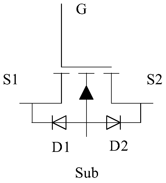
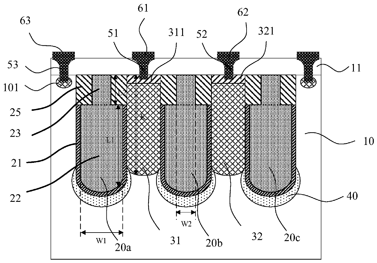
[0071] Figure 2-Figure 4 Respectively show a cross-sectional view and a top view of the bidirectional power device of the first embodiment of the present invention; wherein, figure 2 for Figure 4 Sectional view taken along line AA' in the top view shown, image 3 for Figure 4 Sectional view taken along line BB' in top view shown. In this embodiment, the bidirectional power device is a trench device, which may be a metal oxide semiconductor field effect transistor (MOSFET), an IGBT device or a diode. In the following, an N-type MOSFET is taken as an example for description, however, the present invention is not limited thereto.

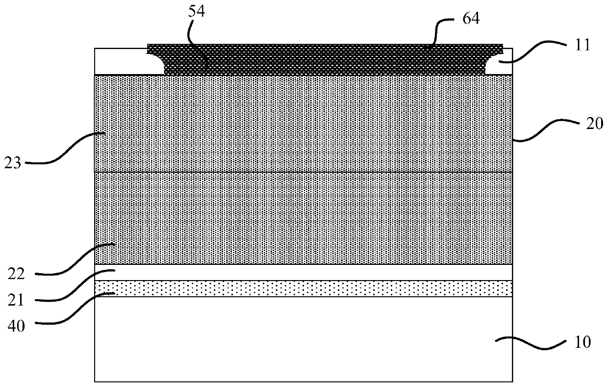
[0072] exist figure 2 The bidirectional power device shown in the figure only contains a schematic diagram of the longitudinal structure of a cell structure, but in actual products, the number of cell structures can be one or more. See Figure 2- Figure 4 , the bidirectional power device includes a semiconductor layer 10, a trench 20 locat...

no. 2 example

[0096] This embodiment adopts basically the same technical solution as the first embodiment, the difference is that in the first embodiment, the third contact 63 is formed on the first surface of the semiconductor layer 10, through the third contact hole 53, the third The lead region 101 is in contact with the semiconductor layer 10 to form a substrate electrode Sub. However, in this embodiment, the third contact 63 is formed on the second surface of the semiconductor layer 10, such as Figure 6 shown. Specifically, a bidirectional power device is formed on a substrate 1 with a higher doping concentration, and then a metal layer is evaporated on the backside of the substrate 1 to form a third contact 63 .

[0097] In the first embodiment, the gate, the substrate electrode, the first output electrode and the second output electrode of the bidirectional power device are drawn from the first surface of the semiconductor layer 10, which is suitable for chip scale packaging (CSP)....

no. 3 example

[0101] This embodiment adopts basically the same technical scheme as the first embodiment. Compared with the first embodiment, this embodiment also includes a wiring layer 70 (not shown in the figure) and a plurality of metal solder balls on the wiring layer 70 80.

[0102] Since the pitch of the trenches 20 is very small, the gate electrodes drawn from the trench structure are relatively narrow, resulting in a large parasitic resistance. In order to reduce parasitic resistance, a wiring layer 70 is added above the power device provided in the first embodiment.

[0103] Such as Figure 7 and Figure 8 As shown, the wiring layer 70 (not shown in the figure) is located on the surface of the power device, and is used to form the first output electrode of the first contact 61, the second contact 62, the third contact 63 and the fourth contact 64. S1, the second output electrode S2, the substrate electrode Sub and the gate electrode G are drawn out to the surface of the power de...


PUM

PropertyMeasurementUnit
Thicknessaaaaaaaaaa
Doping concentrationaaaaaaaaaa
Thicknessaaaaaaaaaa

Abstract

The invention discloses a bidirectional power device and a manufacturing method thereof. The bidirectional power device comprises: a semiconductor layer; a groove located in the semiconductor layer; agate dielectric layer located at the side wall of the groove; a control gate located at the lower portion of the groove; and a shielding gate located at the upper portion of the groove, wherein the control gate is in mutual contact with the shielding gate, and the control gate is separated from the semiconductor layer by the gate dielectric layer. The shielding gate is located on the control gatewhich is in mutual contact with the shielding gate, and is separated from a source and a drain through a shielding dielectric layer, and when the bidirectional power device is cut off, the shieldinggate depletes charges of a second doped region through the shielding dielectric layer, and the voltage-withstanding characteristic is improved. When the bidirectional power device is conducted, the source and/or the drain and the semiconductor layer provide a low-impedance conduction path.

Description

technical field [0001] The invention relates to the technical field of semiconductor manufacturing, in particular to a bidirectional power device and a manufacturing method thereof. Background technique [0002] Power devices are mainly used in high-power power supply circuits and control circuits, such as switching elements or rectifying elements. In power devices, doped regions of different doping types form a PN junction, thereby realizing the function of a diode or a transistor. Power devices are often used in applications that need to carry large currents at high voltages. On the one hand, in order to meet the demands of high-voltage applications and improve device reliability and lifetime, power devices need to have a high breakdown voltage. On the other hand, in order to reduce the power consumption and heat generated by the power device itself, the power device needs to have a low on-resistance. In the power supply circuit, charging and discharging are often invol...

Claims


Application Information

Patent Timeline
IPC IPC(8): H01L29/06H01L29/10H01L29/423H01L29/78
CPCH01L29/4236H01L29/42364H01L29/1033H01L29/0611H01L29/0696H01L29/7831H01L29/7834
Inventor 张邵华
Owner HANGZHOU SILAN MICROELECTRONICS
Why Eureka
Try Eureka