Bidirectional power device and manufacturing method thereof

A bidirectional power device and control gate technology, applied in semiconductor devices, electrical components, circuits, etc., can solve the problems of increasing power consumption and increasing on-resistance, reducing channel length, reducing channel resistance, improving Effect of withstand voltage characteristics

Pending Publication Date: 2019-08-16
HANGZHOU SILAN MICROELECTRONICS
View PDF2 Cites 9 Cited by
  • Summary
  • Abstract
  • Description
  • Claims
  • Application Information

AI Technical Summary

Problems solved by technology

However, due to the reduction of the impurity concentration of the lightly doped

Method used


Image

  • Bidirectional power device and manufacturing method thereof
  • Bidirectional power device and manufacturing method thereof
  • Bidirectional power device and manufacturing method thereof

Examples


no. 1 example

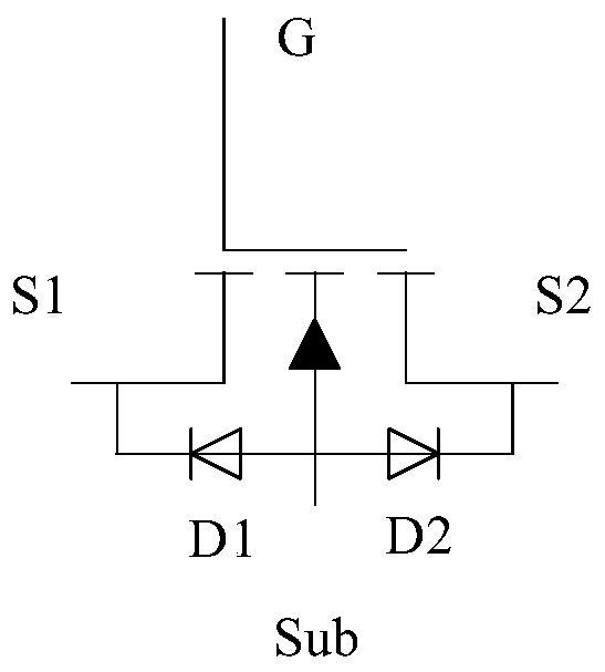
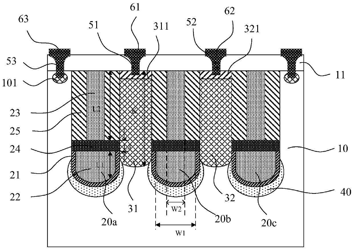
[0075] Figure 2-Figure 4 A cross-sectional view and a top view of the bidirectional power device according to the first embodiment of the present invention are respectively shown; wherein, figure 2 for Figure 4 Sectional view taken along line AA' in the top view shown, image 3 for Figure 4 Sectional view taken along line BB' in top view shown. In this embodiment, the bidirectional power device is a trench device, which may be a metal oxide semiconductor field effect transistor (MOSFET), an IGBT device or a diode. In the following, an N-type MOSFET is taken as an example for illustration, however, the present invention is not limited thereto.

[0076] exist figure 2 The bidirectional power device shown in only contains a schematic diagram of the longitudinal structure of a cell structure, but in actual products, the number of cell structures can be one or more. see Figure 2-Figure 4 , the bidirectional power device includes a semiconductor layer 10, a trench 20 lo...

no. 2 example

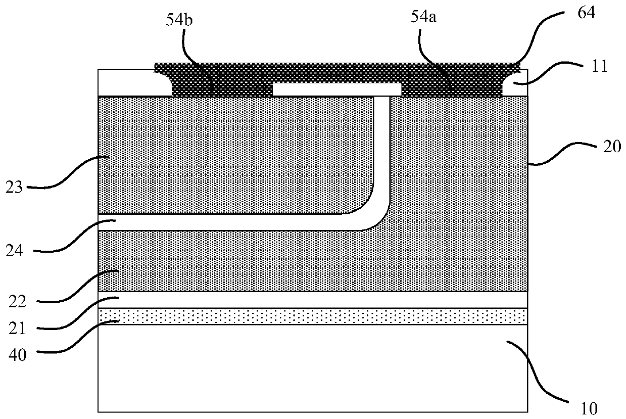
[0101] This embodiment adopts basically the same technical solution as the first embodiment, the difference is that in the first embodiment, the control grid 22 and the shielding grid 23 are connected together, while in this embodiment, the shielding grid 23 and the semiconductor layer 10 connected together, such as Figure 6 As shown, the contact hole 54b of the shielding grid 23 is connected to the contact hole 53 of the substrate electrode, so that the shielding grid 23 and the substrate electrode Sub are electrically connected together.

[0102] In this embodiment, the remaining parts of the bidirectional power device are basically the same as those in the first embodiment, and the specific structure will not be repeated here.

[0103] In the first embodiment, the control gate 22 and the shielding gate 23 are connected together, the shielding gate 23 overlaps with the source region 31 and the drain region 32 , and parasitic capacitance exists. When the voltage of the cont...

no. 3 example

[0106] This embodiment adopts basically the same technical solution as the first embodiment, the difference is that in the first embodiment, the third contact 63 is formed on the first surface of the semiconductor layer 10, through the third contact hole 53, the third The lead region 101 is in contact with the semiconductor layer 10 to form a substrate electrode Sub. However, in this embodiment, the third contact 63 is formed on the second surface of the semiconductor layer 10, such as Figure 7 shown. Specifically, the bidirectional power device is formed on the substrate 1 with a higher doping concentration, and then the metal layer 60 is evaporated on the backside of the substrate 1 to form the third contact 63 .

[0107] In the first embodiment, the gate, the substrate electrode, the first output electrode and the second output electrode of the bidirectional power device are drawn from the first surface of the semiconductor layer 10, which is suitable for chip scale packa...


PUM

PropertyMeasurementUnit
Thicknessaaaaaaaaaa
Doping concentrationaaaaaaaaaa
Thicknessaaaaaaaaaa

Abstract

The invention discloses a bidirectional power device and a manufacturing method thereof. The bidirectional power device comprises: a semiconductor layer; a groove located in the semiconductor layer; agate dielectric layer located at the side wall of the groove; a control gate located at the lower portion of the groove; a shielding gate located at the upper portion of the groove; and an isolationlayer located between the control gate and the shielding gate, wherein the control gate is separated from the semiconductor layer by the gate dielectric layer. The shielding gate is located at the upper portion of the control gate which is mutually separated from the shielding gate, and is separated from a source and a drain through a shielding dielectric layer, and when the bidirectional power device is cut off, the shielding gate depletes charges of a second doped region through the shielding dielectric layer, and the voltage-withstanding characteristic is improved. When the bidirectional power device is conducted, the source and/or the drain and the semiconductor layer provide a low-impedance conduction path.

Description

technical field [0001] The invention relates to the technical field of semiconductor manufacturing, in particular to a bidirectional power device and a manufacturing method thereof. Background technique [0002] Power devices are mainly used in high-power power supply circuits and control circuits, such as switching elements or rectifying elements. In power devices, doped regions of different doping types form a PN junction, thereby realizing the function of a diode or a transistor. Power devices are often required to carry large currents at high voltages in applications. On the one hand, in order to meet the demands of high-voltage applications and improve device reliability and lifetime, power devices need to have a high breakdown voltage. On the other hand, in order to reduce the power consumption and heat generated by the power device itself, the power device needs to have a low on-resistance. In the power supply circuit, charging and discharging are often involved, a...

Claims


Application Information

Patent Timeline
IPC IPC(8): H01L29/06H01L29/10H01L29/423H01L29/78
CPCH01L29/4236H01L29/42364H01L29/1033H01L29/0611H01L29/0696H01L29/7831H01L29/407H01L29/7834H01L29/1041H01L29/423H01L29/66621H01L29/1087
Inventor 张邵华
Owner HANGZHOU SILAN MICROELECTRONICS
Why Eureka
Try Eureka