
Ultra-thin film infrared broadband thermoelectronic photoelectric detector

A technology of photoelectric detectors and thermal electrons, which is applied to photometry, circuits, and electrical components using electric radiation detectors. and polarization-insensitive, easy-to-prepare effects

Inactive Publication Date: 2019-08-16
SUZHOU UNIV +1
View PDF9 Cites 3 Cited by
  • Summary
  • Abstract
  • Description
  • Claims
  • Application Information

AI Technical Summary

Problems solved by technology

[0005] The purpose of the present invention is to provide an ultra-thin film infrared broadband thermoelectron photodetector to solve the problem that the light absorption efficiency of the thermoelectron photodetector is not high

Method used

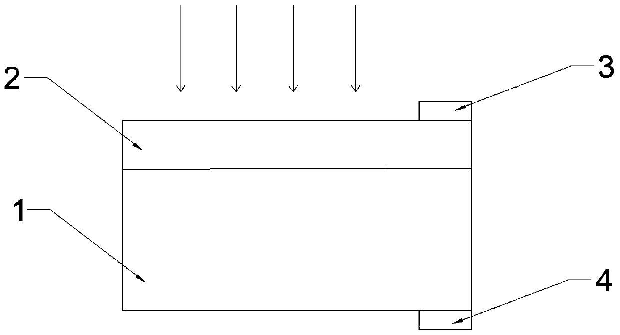

Image

  • Ultra-thin film infrared broadband thermoelectronic photoelectric detector
  • Ultra-thin film infrared broadband thermoelectronic photoelectric detector
  • Ultra-thin film infrared broadband thermoelectronic photoelectric detector

Examples


Embodiment

[0030] Such as Figure 1-4 As shown, an ultra-thin-film infrared broadband thermal electron photodetector is composed of a silicon substrate 1, a metal film 2, a top conductive electrode 3 and a bottom conductive electrode 4, and the upper end of the silicon substrate 1 is a metal The thin film 2, the metal thin film 2 and the silicon substrate 1 are respectively provided with a top conductive electrode 3 and a bottom conductive electrode 4.

[0031] The loss of hot electrons transported to the Schottky interface in metals can be described by an exponential decay model, where L is the transport distance of hot electrons and λ is the mean free path of hot electrons. When the metal thickness is much greater than the mean free path, the generated hot electrons will be lost in thermalization before reaching the Schottky interface, resulting in no current generation in the system. Compared with the traditional thermal electron photodetector, the technical proposal constructs a met...


PUM

PropertyMeasurementUnit
Thicknessaaaaaaaaaa

Abstract

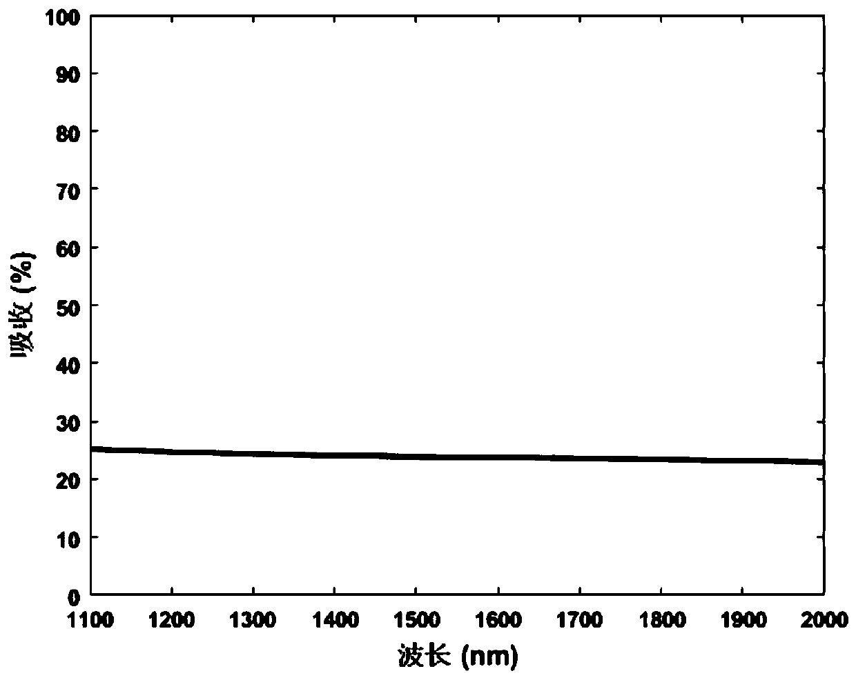
The invention discloses an ultra-thin film infrared broadband thermoelectronic photoelectric detector, which is composed of a silicon substrate, a metal film, a top conductive electrode and a bottom conductive electrode. The metal film is arranged on the upper end of the silicon substrate. The top conductive electrode and the bottom conductive electrode are respectively arranged on one side of themetal film and on one side of the silicon substrate. The beneficial effects of the invention are as follows: a metal material with infrared broadband absorption property is used as an absorption layer, and a planar film with thickness of only few tens of nanometers can absorb more than 20% of light; the metal film is extremely thin, and the thickness of the metal film is equivalent to the averagefree path of hot electrons, so that the transport efficiency of hot electrons and the response of the photoelectric detector are greatly improved; and the Schottky barriers of the metal and the semiconductor can be adjusted by a contact interface and a device technology to achieve broadband detection in the infrared band. The photoelectric detector is only composed of a metal film and a semiconductor substrate and is quite simple in structure, so that the photoelectric detector is easy to prepare, suitable for mass production and has high yield.

Description

technical field [0001] The invention relates to the field of electronic optoelectronic technology, in particular to an ultra-thin-film infrared broadband thermal electron photodetector. Background technique [0002] The working principle of traditional silicon-based photodetectors is: when the incident photon energy is higher than the semiconductor band gap, the valence band electrons in silicon absorb photons and then transition to the conduction band to generate photogenerated carriers, and then pass through the PN junction and Schottky junction. Or the separation of photogenerated carriers such as tunnel junctions to realize photodetection. However, since silicon materials are transparent to infrared bands with energy lower than the bandgap, silicon photodetectors have bandwidth limitations and cannot achieve photodetection in this band [Nanophotonics, 2016, 5(1):96-111]. [0003] Since metal has no band gap, the hot electrons excited by metal absorption of photons (elec...

Claims


Application Information

Patent Timeline
IPC IPC(8): H01L31/108G01J1/42
CPCG01J1/42H01L31/108
Inventor 李孝峰张程吴绍龙丁浩李亮乔文陈林森
Owner SUZHOU UNIV
Learn More