Supercharge Your Innovation With Domain-Expert AI Agents!

Preparation method of silicon-copper composite nanowire

A nanowire and silicon-copper technology, which is applied in the field of preparation of silicon-copper composite nanowires, can solve the problems of high cost and poor uniformity, and achieve the effect of overcoming the difficulty of in-situ compounding, high conductivity, and uniform distribution of elements

Active Publication Date: 2019-08-23
南京卓胜自动化设备有限公司
View PDF9 Cites 3 Cited by
  • Summary
  • Abstract
  • Description
  • Claims
  • Application Information

AI Technical Summary

Problems solved by technology

At present, the compounding of silicon and metal materials mainly adopts methods such as coating and multi-element metal corrosion, but the cost is high and the uniformity is poor. The work of using silicon-copper in-situ compounding method to prepare silicon-copper composite nanowires has not yet been reported.

Method used


Image

  • Preparation method of silicon-copper composite nanowire
  • Preparation method of silicon-copper composite nanowire
  • Preparation method of silicon-copper composite nanowire

Examples


Embodiment 1

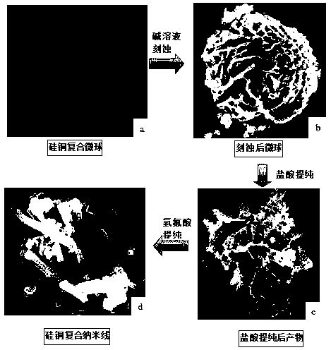
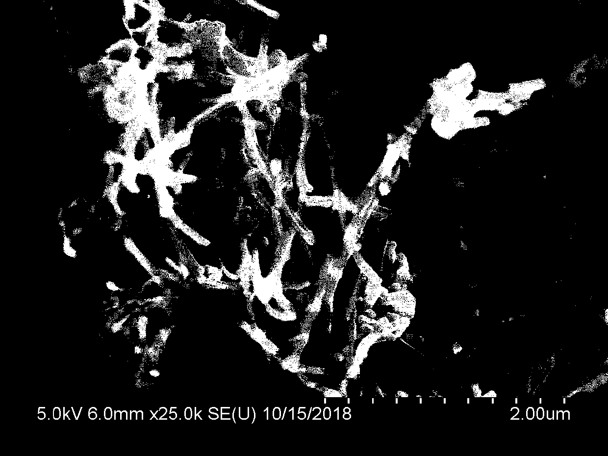
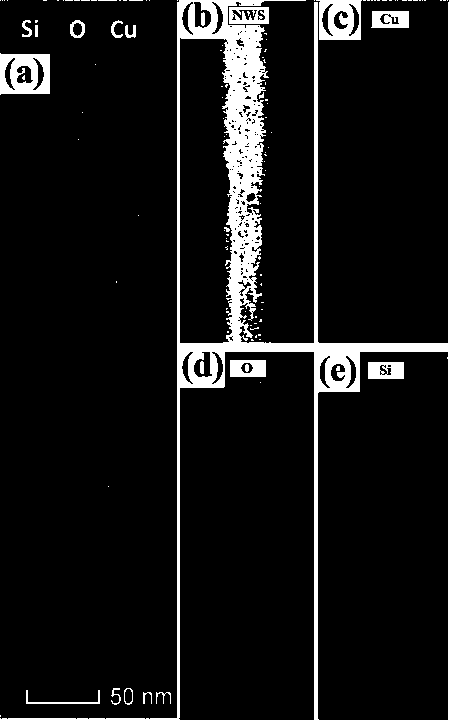
[0037] This embodiment provides a method for preparing silicon-copper composite nanowires using silicon-copper composite microspheres. When silicon-copper composite microspheres are used as raw materials, chemical etching and purification are used to prepare silicon-copper composite nanowires. The specific steps are as follows:

[0038] 1) Select P-type single crystal silicon master alloy with electrical conductivity of 0.01~0.015Ω·cm as the raw material, and process it by pulse discharge method. The processing parameters are: open circuit voltage 120V; peak current 5A; pulse width 50µs; duty ratio 1:2 , the working fluid is deionized water, and the electrode is copper electrode. Process and collect doped silicon-copper composite microspheres. The particle size range of silicon-copper composite microspheres is 1-5µm, the size is concentrated at 3µm, and the concentration is greater than 90%.

[0039] 2) Measure 10g of silicon-copper composite microspheres as the matrix materia...

Embodiment 2

[0050] This embodiment provides a method for preparing silicon-copper composite nanowires using silicon-copper composite microspheres. When silicon-copper composite microspheres are used as raw materials, chemical etching and purification are used to prepare silicon-copper composite nanowires. The specific steps are as follows:

[0051] 1) Select P-type single crystal silicon master alloy with electrical conductivity of 0.01~0.015Ω·cm as the raw material, and process it by pulse discharge method. The processing parameters are: open circuit voltage 120V; peak current 5A; pulse width 50µs; duty ratio 1:2 , the working fluid is deionized water, and the electrode is copper electrode. Process and collect doped silicon-copper composite microspheres. The particle size range of silicon-copper composite microspheres is 1-5µm, the size is concentrated at 3µm, and the concentration is greater than 90%.

[0052] 2) Measure 10g of silicon-copper composite microspheres as the matrix materia...

Embodiment 3

[0063] This embodiment provides a method for preparing silicon-copper composite nanowires using silicon-copper composite microspheres. When silicon-copper composite microspheres are used as raw materials, chemical etching and purification are used to prepare silicon-copper composite nanowires. The specific steps are as follows:

[0064] 1) Select P-type single crystal silicon master alloy with electrical conductivity of 0.01~0.015Ω·cm as the raw material, and process it by pulse discharge method. The processing parameters are: open circuit voltage 120V; peak current 5A; pulse width 50µs; duty ratio 1:2 , the working fluid is deionized water, and the electrode is copper electrode. Process and collect doped silicon-copper composite microspheres. The particle size range of silicon-copper composite microspheres is 1-5µm, the size is concentrated at 3µm, and the concentration is greater than 90%.

[0065] 2) Measure 10g of silicon-copper composite microspheres as the matrix materia...


PUM

PropertyMeasurementUnit
Particle sizeaaaaaaaaaa
Lengthaaaaaaaaaa

Abstract

The invention discloses a preparation method of a silicon-copper composite nanowire. The method comprises the following steps: selecting a silicon-copper composite microsphere in a certain size as a raw material, etching a silicon element in an alkaline solution under the action of ultrasonic waves, performing cleaning, and then soaking the silicon-copper composite microsphere in an acidic solution to remove copper oxide, performing cleaning again, soaking the silicon-copper composite microsphere in another acid solution to remove silicon dioxide, and performing cleaning to obtain the silicon-copper composite nanowire. The whole preparation method is reasonable in process design, high in operability, low in production cost, high in production efficiency and capable of achieving large-scaleindustrial production. The prepared silicon-copper composite nanowire is compact in structure and uniform in element distribution, and can be widely applied to the fields of lithium batteries, solarcells, semiconductors, sensors and the like.

Description

technical field [0001] The invention relates to the field of preparation of a composite nanomaterial, in particular to a method of chemically etching a silicon-copper composite microsphere through an alkaline solution under certain reaction conditions, and then purifying it with an acidic solution to prepare a compound with controllable structure and components. Preparation method of silicon-copper composite nanowires. Background technique [0002] Nanomaterials, such as nanowires, nanotubes, nanorods, etc., have attracted extensive attention of material scientists. Silicon-based composite nanomaterials have attracted much attention in recent years in the fields of various detectors, biological microsensors, optoelectronic nano-devices, energy storage materials, etc., especially as anode materials for lithium batteries. [0003] Compared with traditional anode materials, silicon has an ultra-high theoretical specific capacity and lower delithiation potential, but the disadv...

Claims


Application Information

Patent Timeline
IPC IPC(8): H01M4/36H01M4/38H01M10/0525B82Y30/00
CPCB82Y30/00H01M4/362H01M4/38H01M4/386H01M10/0525H01M2004/027Y02E60/10
Inventor 洪捐杨晓芳耿其东周兆峰杜建周
Owner 南京卓胜自动化设备有限公司
Features
  • R&D
  • Intellectual Property
  • Life Sciences
  • Materials
  • Tech Scout
  • Unparalleled Data Quality
  • Higher Quality Content
  • 60% Fewer Hallucinations
Learn More