

Electron transport layer ink, preparation method thereof and electroluminescence device
An electron transport layer and ink technology, which is applied to electric solid devices, electrical components, semiconductor devices, etc., can solve the problems of device preparation difficulties, and achieve the effects of simple preparation method, suppression of damage, and enhancement of electron injection and transmission capabilities.
- Summary
- Abstract
- Description
- Claims
- Application Information
AI Technical Summary
Problems solved by technology
Method used
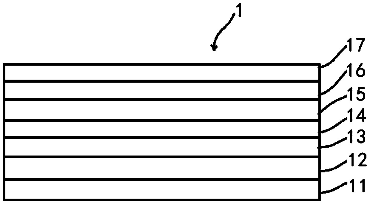
Image

Examples
Embodiment 1
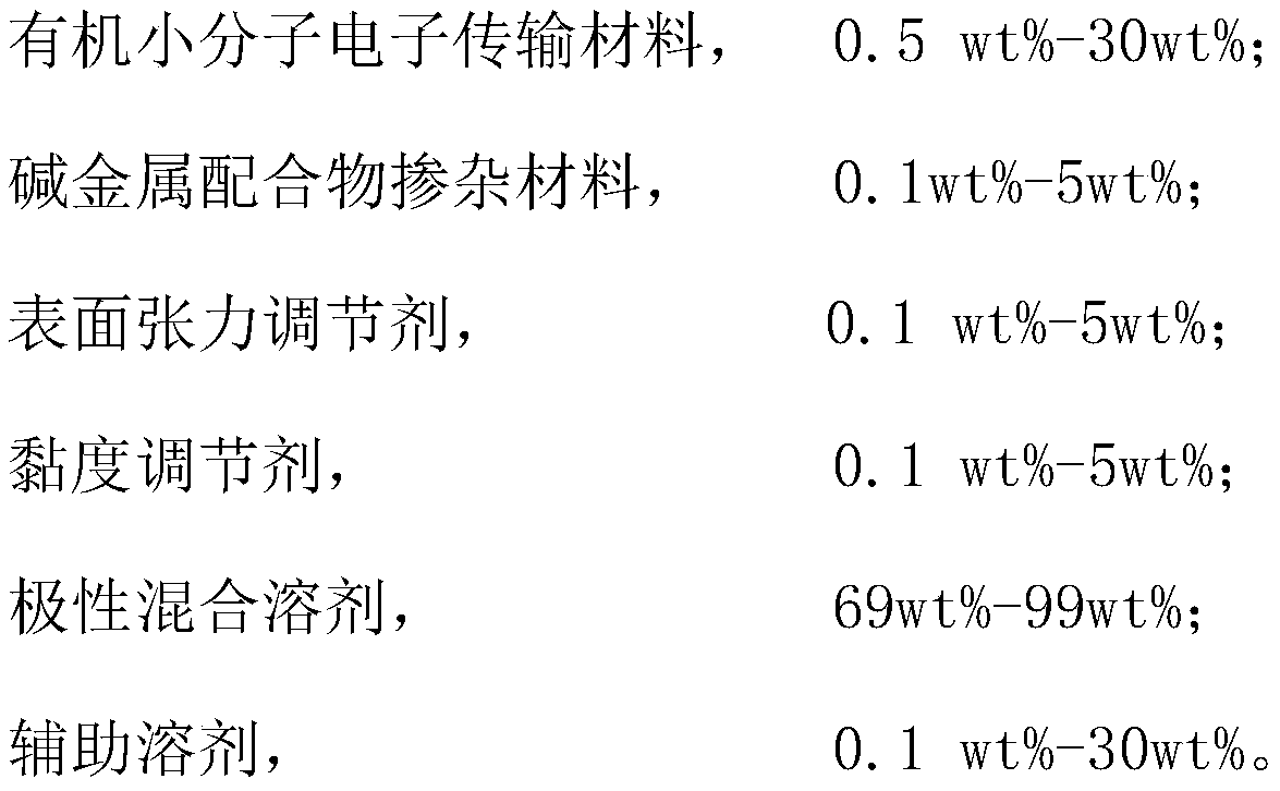
[0032] The electronic transport layer ink of the present invention, its components include organic small molecule electron transport material, 30wt%; alkali metal complex doping material, 0.1wt%; surface tension regulator, 0.1wt%; viscosity regulator , 0.1wt%; polar mixed solvent, 69wt%; auxiliary solvent, 0.7wt%.
[0033] 2,2'-(1,3-phenyl)bis[5-(4-tert-butylphenyl)-1,3,4-oxadiazole] is selected as the small organic molecule electron transport material. The alkali metal complex doping material is lithium 8-hydroxyquinolate. In the surface tension modifier, dimethylformamide is selected as a co-solvent, sodium alkylbenzenesulfonate as a surfactant, and hydroquinone as a small molecule compound for regulating surface tension;
[0034] The viscosity regulator is selected from amine compounds. The polar mixed solvent is a polyalcohol compound, and ethylene glycol is selected in this embodiment. The auxiliary solvent is selected from amide compounds.
[0035] This embodiment al...
Embodiment 2
[0037]The electronic transport layer ink of the present invention, its components include organic small molecule electron transport material, 10wt%; alkali metal complex doping material, 2wt%; surface tension regulator, 2wt%; viscosity regulator, 2wt% by weight percentage. %; polar mixed solvent, 80wt%; auxiliary solvent, 4wt%.
[0038] 1,3,5-tris(1-phenyl-benzo[D]pyrazol-2-yl)benzene is selected as the small organic molecule electron transport material. The alkali metal complex doping material is lithium 8-hydroxyquinolate.
[0039] In the surface tension regulator, cyclohexane is used as a co-solvent, sodium alkylbenzenetripolyethylene sulfonate is used as a surfactant, and imidazole and its derivatives are small molecular compounds for regulating surface tension.
[0040] The viscosity regulator is selected from ether compounds. The polar mixed solvent is a polyalcohol compound, and ethylene glycol is selected in this embodiment. The auxiliary solvent is selected from et...
Embodiment 3
[0043] The electron transport layer ink of the present invention, its component comprises organic small molecule electron transport material, 5wt% by weight percentage; Alkali metal complex doping material, 5wt%; Surface tension regulator, 5wt%; Viscosity regulator, 5wt% %; polar mixed solvent, 69wt%; auxiliary solvent, 11wt%.
[0044] 2,2'-(1,3-phenyl)bis[5-(4-tert-butylphenyl)-1,3,4-oxadiazole] is selected as the small organic molecule electron transport material. The alkali metal complex doping material is lithium 8-hydroxyquinolate. In the surface tension modifier, dimethylformamide is selected as a co-solvent, sodium alkylbenzenesulfonate as a surfactant, and hydroquinone as a small molecule compound for regulating surface tension;
[0045] The viscosity regulator is selected from amine compounds. The polar mixed solvent is a polyalcohol compound, and ethylene glycol is selected in this embodiment. The auxiliary solvent is selected from amide compounds.
[0046] Tests...
PUM
 Abstract
Description
Claims
Application Information