Silicon-based lithium niobate thin film electro-optic modulator array

An electro-optical modulator, silicon-based lithium niobate technology, applied in the directions of light guides, optics, instruments, etc., can solve the problems of reducing the conversion rate of electro-optical modulation, low modulation efficiency of doped silicon, and high half-wave voltage, so as to ensure functional effectiveness. and stability, improving preparation efficiency, and the effect of ultra-high modulation bandwidth

Inactive Publication Date: 2019-08-30
SHANGHAI JIAO TONG UNIV
View PDF6 Cites 12 Cited by
  • Summary
  • Abstract
  • Description
  • Claims
  • Application Information

AI Technical Summary

Problems solved by technology

However, the use of doped silicon as a light-guiding medium has the following problems: doped silicon has an absorption effect on light, which will significantly increase the insertion loss of the electro-optic modulator; the modulation efficiency of doped silicon is low, so the designed hal...

Method used


Image

  • Silicon-based lithium niobate thin film electro-optic modulator array
  • Silicon-based lithium niobate thin film electro-optic modulator array
  • Silicon-based lithium niobate thin film electro-optic modulator array

Examples


Embodiment Construction

[0037] The technical solutions of the present invention will be described in detail below in conjunction with the accompanying drawings and examples, and detailed implementation methods and structures are given, but the scope of protection of the present invention is not limited to the following examples.

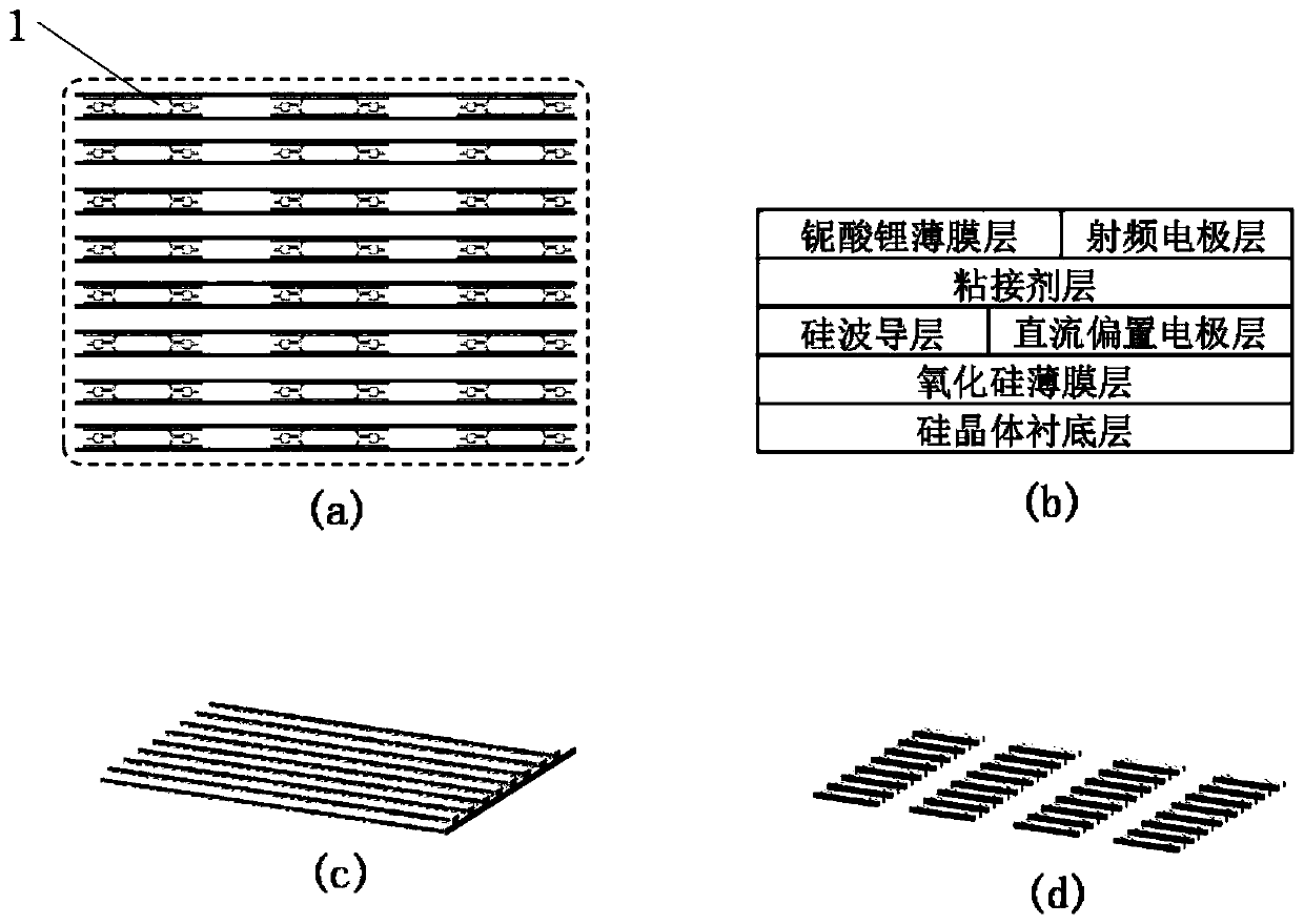
[0038] see figure 1 , the figure depicts a part of a large-scale silicon-based lithium niobate thin film electro-optic modulator array at the wafer level. It can be seen from the top view that multiple silicon-based lithium niobate thin film electro-optic modulators 1 are fabricated on one wafer at the same time. As can be seen from the schematic diagram of the longitudinal section, the silicon-based lithium niobate thin film electro-optic modulator array proposed by the present invention comprises a silicon crystal substrate layer, a silicon oxide thin film layer, a silicon waveguide layer, an adhesive layer, a lithium niobate thin film layer, a DC bias The electrode laye...


PUM


Abstract

The invention relates to a large-scale silicon-based lithium niobate thin film electro-optic modulator array. The invention has the advantages that the difficulty of preparation process of a lithium niobate crystal layer is reduced through a structural design, the precision requirement of bonding of lithium niobate and silicon is reduced, the preparation and the bonding of a large-scale array typelithium niobate crystal layer can be simultaneously completed at one time, and the production efficiency of the silicon-based lithium niobate thin film electro-optic modulator array is greatly improved; and through the structural design and optimization of the silicon crystal layer, light can be naturally alternated and transmitted mutually in silicon waveguide and lithium niobate waveguide, anda high-performance lithium niobate thin film electro-optic modulation effect is realized. In addition, the method utilizes the maturity advantage of a standardized silicon-based integration technologyand concentrates a complex chip preparation process on the silicon crystal layer, thereby reducing the process error in the chip manufacturing process and ensuring the performance stability of the whole silicon-based lithium niobate thin film electro-optic modulator array.

Description

technical field [0001] The invention relates to the technical field of optoelectronic integrated devices, in particular to a large-scale silicon-based lithium niobate thin-film electro-optical modulator array. [0002] technical background [0003] The electro-optic modulator loads the electrical signal onto the optical signal, and is the signal input interface of optical signal processing systems such as optical communication and microwave photonic radar. Its performance directly determines the performance of the optical signal processing system, so it has become a very important photonic device. In order to realize an integrated electro-optic modulator on a chip, an electro-optic modulator using a standardized silicon-based integration process has appeared (Ding Jianfeng, Zhang Lei, Yang Lin, "Silicon-based integrated differential electro-optic modulator and its preparation method", national invention patent CN105044931B , 2015). Using doped silicon as the light-guiding m...

Claims


Application Information

Patent Timeline
IPC IPC(8): G02F1/035G02B6/132G02B6/136G02B6/12G02B6/125
CPCG02B6/12G02B6/125G02B6/132G02B6/136G02B2006/1204G02B2006/12142G02B2006/12159G02B2006/12176G02F1/035
Inventor 邹卫文徐绍夫王静陈建平
Owner SHANGHAI JIAO TONG UNIV
Why Eureka
Try Eureka