

Gallium nitride crystal growth apparatus and gallium nitride crystal growth method
A crystal growth and gallium nitride technology, applied in crystal growth, single crystal growth, single crystal growth, etc., can solve problems such as uneven crystal thickness, raw material loss, and low crystal quality, so as to reduce raw material loss and improve growth Effects of speed and crystallization quality
- Summary
- Abstract
- Description
- Claims
- Application Information
AI Technical Summary
Problems solved by technology
Method used
Image

Examples
no. 1 approach
[0041] The following is based on Figure 2 to Figure 3 A first embodiment of the gallium nitride crystal growth apparatus according to the present invention will be described in detail.
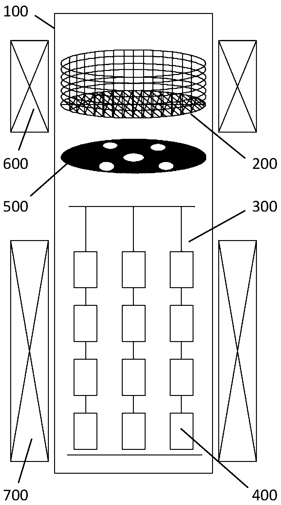
[0042] In this embodiment, if figure 2 As shown, the gallium nitride crystal growth device according to the present invention includes a reaction vessel 1 , a raw material area 2 , a crystallization area 3 , a partition 4 and a heating device assembly 5 .
[0043] In the present embodiment, the reaction vessel 1 has a substantially cylindrical shape as a whole, and the reaction vessel 1 is filled with liquid ammonia.
[0044] The raw material area 2 includes a first raw material area 21 and a second raw material area 22, and each raw material area 2 is provided with a raw material basket 23 for accommodating polycrystalline compost.
[0045] The crystallization region 3 includes a first crystallization region 31 , a second crystallization region 32 and a third crystallization region 33 . ...
no. 2 approach
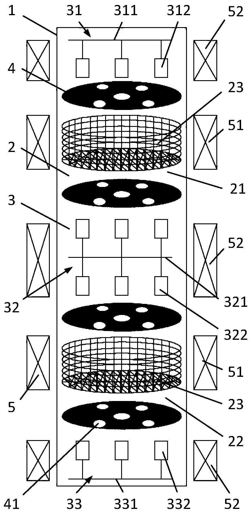
[0062] The following is based on Figure 4 A second embodiment of the gallium nitride crystal growth apparatus according to the present invention will be described in detail.
[0063] In this embodiment, if Figure 4 As shown, the gallium nitride crystal growth apparatus according to the present invention includes a reaction vessel 10 , a raw material area 20 , a crystallization area 30 , a partition 40 and a heating device assembly 50 .
[0064] The configurations of the reaction vessel 10 , the separator 40 and the heater unit 50 in this embodiment are substantially the same as those of the reaction vessel 1 , the separator 4 and the heater unit 5 in the first embodiment.
[0065] In this embodiment, if Figure 4 As shown, the raw material zone 20 includes a third raw material zone 201 , a fourth raw material zone 202 and a fifth raw material zone 203 . Each raw material area 20 is provided with a raw material basket 204 for accommodating polycrystalline compost.
[0066...
PUM
 Abstract
Description
Claims
Application Information