Physical vapor deposition (PVD) flexible conducting film, preparation method, and method for generating microcircuit through nanometer effect

A flexible conductive and nano-effect technology, applied in circuits, conductive layers on insulating carriers, semiconductor/solid-state device manufacturing, etc., can solve problems such as high cost, inability to make special-shaped circuits, and scrapped finished circuits.

Inactive Publication Date: 2019-09-06
贵州优宝泰光电有限责任公司
View PDF6 Cites 3 Cited by
  • Summary
  • Abstract
  • Description
  • Claims
  • Application Information

AI Technical Summary

Problems solved by technology

[0004] The purpose of the present invention is to: for the above-mentioned existing microcircuit generation technology is to generate circuits and integrated circuits through molds and templates, it cannot make special-shaped circuits, and when a certain circuit point or a certain section of the circuit is damaged in the finished circuit, the entire finished circuit It will be scrapped and the cost is high. The present invention provides a PVD flexible conductive film, a preparation method and a method for generating microcircuits through nano-effects.

Method used


Image

  • Physical vapor deposition (PVD) flexible conducting film, preparation method, and method for generating microcircuit through nanometer effect

Examples


preparation example Construction

[0032] A preparation method for a PVD flexible conductive film, comprising the following steps:

[0033] (1) Using the physical vapor deposition (PVD) vacuum evaporation method, in a vacuum environment, the base layer material is evaporated into vapor phase deposition on the substrate to form the base layer 1;

[0034] (2) melting and mixing the conductive material;

[0035] (3) Using the physical vapor deposition (PVD) sputtering coating method, in a vacuum environment, through the joint action of voltage and magnetic field, the conductive material is bombarded with ionized inert gas ions, so that the conductive material is ionized in the form of ions It is sputtered out and deposited on the base layer 1 to form a conductive layer 2, thereby preparing a flexible conductive film.

[0036] Further, the evaporation source used for evaporation in the step (1) is resistance heating, electron beam heating, laser heating, high frequency induction heating or arc heating.

[0037] F...

Embodiment 1

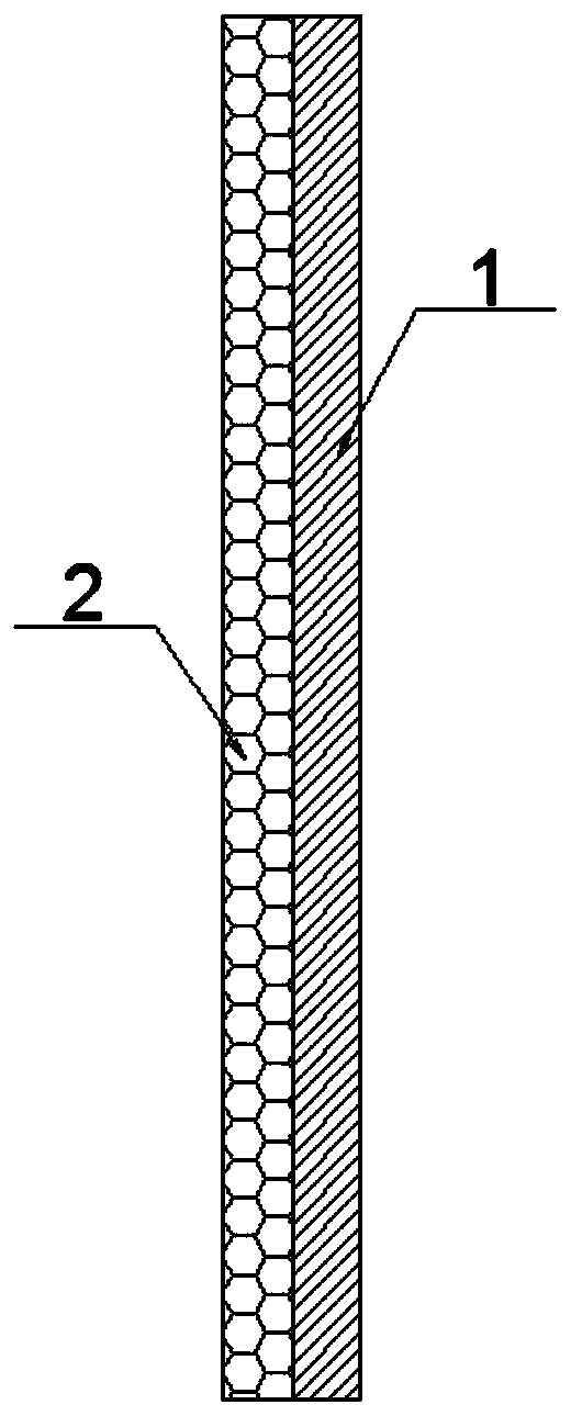
[0047] A PVD flexible conductive film includes a base layer 1 and a conductive layer 2 deposited on the base layer.

[0048] Further, the material of the base layer 1 is indium tin oxide.

[0049] Further, the material of the conductive layer 2 is a mixture of gold and tin.

[0050] A preparation method for a PVD flexible conductive film, comprising the following steps:

[0051] (1) Using the physical vapor deposition (PVD) vacuum evaporation method, in a vacuum environment, the base layer material is evaporated into vapor phase deposition on the substrate to form the base layer 1;

[0052] (2) melting and mixing the conductive material;

[0053] (3) Using the physical vapor deposition (PVD) sputtering coating method, in a vacuum environment, through the joint action of voltage and magnetic field, the conductive material is bombarded with ionized inert gas ions, so that the conductive material is ionized in the form of ions It is sputtered out and deposited on the base laye...

Embodiment 2

[0065] A PVD flexible conductive film includes a base layer 1 and a conductive layer 2 deposited on the base layer.

[0066] Further, the material of the base layer 1 is zinc oxide.

[0067] Further, the material of the conductive layer 2 is a mixture of gold and tin.

[0068] A preparation method for a PVD flexible conductive film, comprising the following steps:

[0069] (1) Using the physical vapor deposition (PVD) vacuum evaporation method, in a vacuum environment, the base layer material is evaporated into vapor phase deposition on the substrate to form the base layer 1;

[0070] (2) melting and mixing the conductive material;

[0071] (3) Using the physical vapor deposition (PVD) sputtering coating method, in a vacuum environment, through the joint action of voltage and magnetic field, the conductive material is bombarded with ionized inert gas ions, so that the conductive material is ionized in the form of ions It is sputtered out and deposited on the base layer 1 to...


PUM


Abstract

The invention discloses a physical vapor deposition (PVD) flexible conducting film, a preparation method, and a method for generating a microcircuit through a nanometer effect. The method for generating the microcircuit by the PVD flexible conducting film through the nanometer effect comprises the following steps of (1) attaching one surface of a conducting layer of the prepared flexible conducting film to the surface of a circuit of a circuit product to be processed; (2) using a charge coupled device (CCD) fitted for a laser device for detect a damaged or missed circuit on a finished-productcircuit; (3) inputting a circuit diagram to be generated into equipment of the laser device; and (4) using the laser device for enabling the conducting layer of the prepared flexible conducting film to emit ions according to the circuit diagram, attaching the ions onto a corresponding circuit position on the circuit product, and repairing the damaged or missed circuit on the finished-product circuit. No mold needs to be used, only the circuit diagram to be generated needs to be input into equipment of the laser device, a circuit of a special-shaped product can be directly generated, and a defective circuit can be repaired.

Description

technical field [0001] The invention relates to the technical field of PVD nano-effects, in particular to a PVD flexible conductive film, a preparation method and a method for generating microcircuits through nano-effects. Background technique [0002] A microcircuit refers to a microelectronic device that has high-density equivalent circuit elements and components and can be used as an independent piece. A microcircuit can be a micro-organization, an integrated circuit, or an integrated microcircuit. [0003] At present, the existing microcircuit generation technology is to generate circuits and integrated circuits through molds and templates, which cannot make special-shaped circuits, and when a certain circuit point or a certain section of the finished circuit is damaged, the entire finished circuit will be scrapped, which is expensive. Contents of the invention [0004] The purpose of the present invention is to: for the above-mentioned existing microcircuit generation...

Claims


Application Information

Patent Timeline
IPC IPC(8): C23C14/24C23C14/02C23C14/06C23C14/08C23C14/18C23C14/35H01B5/14H01L21/02
CPCC23C14/024C23C14/0605C23C14/086C23C14/185C23C14/24C23C14/35H01B5/14H01L21/02
Inventor 郑树伟
Owner 贵州优宝泰光电有限责任公司
Why Eureka
Try Eureka