Preparation method of surface acoustic wave sensor, and prepared sensor and application thereof
A surface acoustic wave and sensor technology, which is applied in the use of sound waves/ultrasonic waves/infrasonic waves to analyze fluids, use sound waves/ultrasonic waves/infrasonic waves for material analysis, and instruments, etc. It can solve the problems of reducing success rate, damage, and secondary pollution of SAW sensors. , to achieve a good nanoscale, improve the preparation efficiency, and improve the effect of utilization
- Summary
- Abstract
- Description
- Claims
- Application Information
AI Technical Summary
Problems solved by technology
Method used
Image

Examples
Embodiment 1
[0021] A preparation method of a surface acoustic wave sensor, the steps are as follows:
[0022] S1. Preparation of SAW chip: select piezoelectric substrate, and prepare interdigital electrodes on the piezoelectric substrate through photolithography and micromachining process;
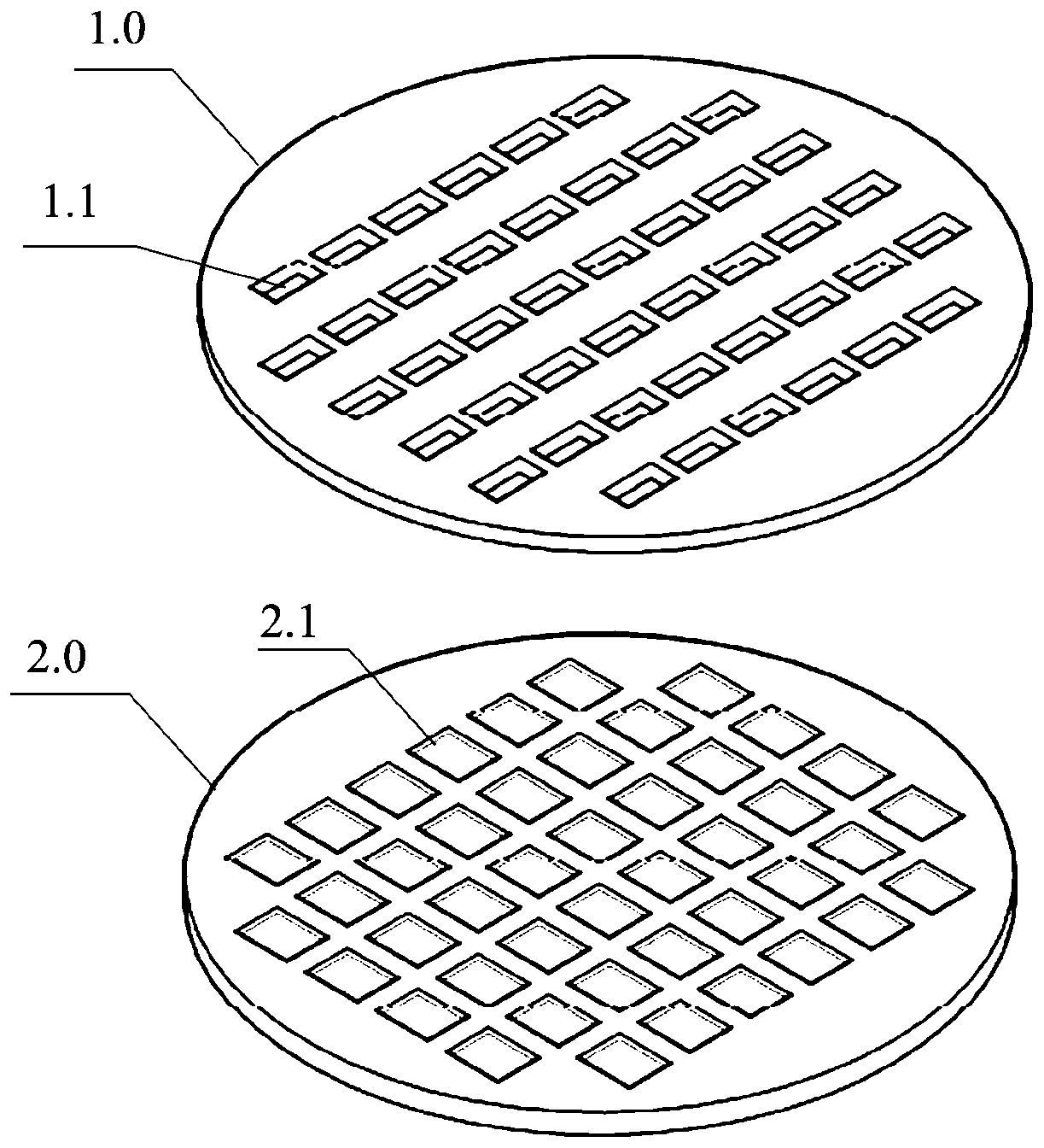
[0023] S2. Preparation of a magnetron sputtering mold: the magnetron sputtering mold is connected by bolts or magnetically by an upper mold and a lower mold; the lower mold is provided with an array of SAW chip card slots in which SAW chips can be placed, and the upper mold is provided with The multiple rectangular through holes corresponding to the delay line area of the SAW chip; the mold prepared in this example is as figure 1 As shown in the figure, 1.0 is the upper mold, 1.1 is the rectangular through hole corresponding to the SAW chip delay line area (the area of the delay line area is 8.4×4.3mm 2 ), 2.0 is the lower mold, 2.1 is the SAW chip card slot array that can place the SAW chip.
[0024] S3...
Embodiment 2
[0034] A preparation method of a surface acoustic wave sensor, the steps are as follows:
[0035] S1. Preparation of SAW chip: select piezoelectric substrate, and prepare interdigital electrodes on the piezoelectric substrate through photolithography and micromachining process;
[0036] S2. Preparation of a magnetron sputtering mold: the magnetron sputtering mold is connected by bolts or magnetically by an upper mold and a lower mold; the lower mold is provided with an array of SAW chip card slots in which SAW chips can be placed, and the upper mold is provided with The multiple rectangular through holes corresponding to the delay line area of the SAW chip; the mold prepared in this example is as figure 1 As shown in the figure, 1.0 is the upper mold, 1.1 is the rectangular through hole corresponding to the SAW chip delay line area (the area of the delay line area is 8.4×4.3mm 2 ), 2.0 is the lower mold, 2.1 is the SAW chip card slot array that can place the SAW chip.
[0037] S3...
Embodiment 3
[0042] A preparation method of a surface acoustic wave sensor, the steps are as follows:
[0043] S1. Preparation of SAW chip: select piezoelectric substrate, and prepare interdigital electrodes on the piezoelectric substrate through photolithography and micromachining process;
[0044] S2. Preparation of a magnetron sputtering mold: the magnetron sputtering mold is connected by bolts or magnetically by an upper mold and a lower mold; the lower mold is provided with an array of SAW chip card slots in which SAW chips can be placed, and the upper mold is provided with The multiple rectangular through holes corresponding to the delay line area of the SAW chip; the mold prepared in this example is as figure 1 As shown in the figure, 1.0 is the upper mold, 1.1 is the rectangular through hole corresponding to the SAW chip delay line area (the area of the delay line area is 8.4×4.3mm 2 ), 2.0 is the lower mold, 2.1 is the SAW chip card slot array that can place the SAW chip.
[0045] S3...
PUM
| Property | Measurement | Unit |
|---|---|---|
| Width | aaaaa | aaaaa |
| Thickness | aaaaa | aaaaa |
Abstract
Description
Claims
Application Information
PatSnap Eureka turns technology decisions into work you can execute. Powered by our Innovation Knowledge Graph, it runs expert workflows across engineering, life sciences, materials and intellectual property. Get your review-ready output in minutes.


