Quantum dot light emitting diode and preparation method thereof and display device
A quantum dot light-emitting and diode technology, applied in the direction of electric solid-state devices, semiconductor devices, organic semiconductor devices, etc., can solve the problems of exciton quenching, lower device performance, high device voltage, etc., achieve enhanced injection, improved performance, and reduced drive The effect of voltage
- Summary
- Abstract
- Description
- Claims
- Application Information
AI Technical Summary
Problems solved by technology
Method used
Image

Examples
preparation example Construction
[0068] The embodiment of the present invention discloses a method for preparing a quantum dot light-emitting diode, comprising the following steps:
[0069] forming a first electron transport layer on the hole transport layer of the quantum dot light emitting diode;
[0070] forming a quantum dot light-emitting layer on the first electron transport layer; and / or
[0071] A quantum dot light emitting layer is formed on the hole transport layer of the quantum dot light emitting diode, and the quantum dot light emitting layer includes quantum dots and doped electron transport materials.
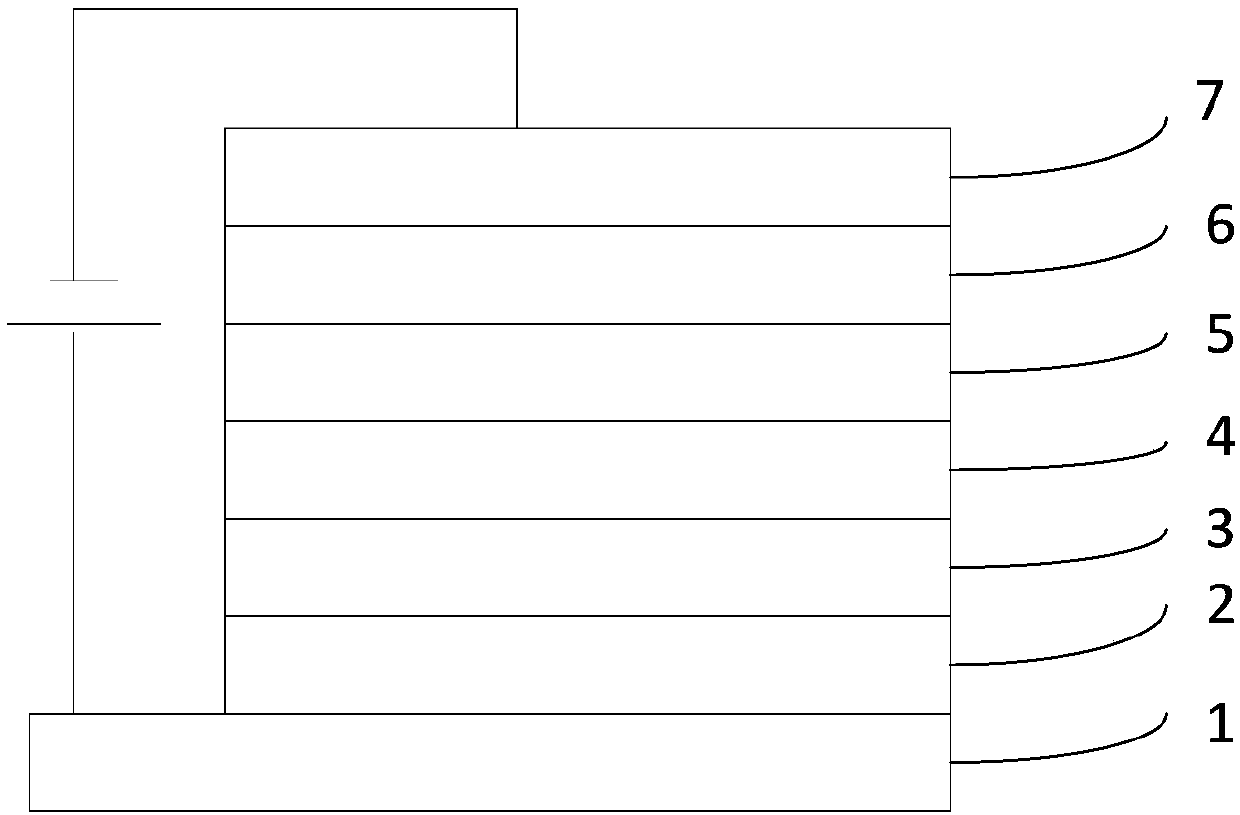
[0072] When the quantum dot light-emitting diode includes an anode, a hole injection layer, the hole transport layer, the first electron transport layer, the quantum dot light-emitting layer, a second electron transport layer and a cathode stacked in layers, the The preparation method of the quantum dot light-emitting diode specifically includes:
[0073] depositing an anode on the substrate; ...
Embodiment 1
[0094] A substrate is provided, and an ITO anode is prepared on the substrate; the ITO anode is sequentially cleaned with acetone, isopropanol, detergent, deionized water, isopropanol, dried and then O 2 Plasma treatment or UV ozone cleaning treatment;
[0095] On the ITO anode, prepare the hole injection layer of PEDOT:PSS material with solution or evaporation method;
[0096] Forming the first sub-hole transport layer of poly-TPD and the second sub-hole transport layer made of PVK by solution or evaporation method;
[0097] The first electron transport layer of B3PYMPM is formed by solution or evaporation method; the thickness of the first electron transport layer is less than 3nm;
[0098] Preparation of quantum dot luminescent layer by solution method;
[0099] Forming the second electron transport layer of ZnO by solution or evaporation method;
[0100] Al electrodes are formed by vapor deposition to obtain quantum dot light-emitting diodes.
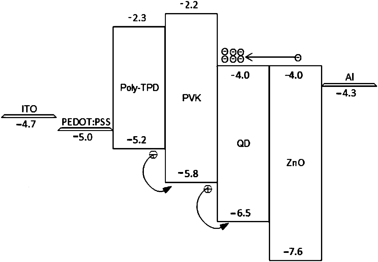
[0101] Figure 5 Schema...
Embodiment 2
[0107] A substrate is provided, and an ITO anode is prepared on the substrate; the ITO anode is sequentially cleaned with acetone, isopropanol, detergent, deionized water, isopropanol, dried and then O 2 Plasma treatment or UV ozone cleaning treatment;
[0108] On the ITO anode, prepare the hole injection layer of PEDOT:PSS material with solution or evaporation method;
[0109] Forming the first sub-hole transport layer of poly-TPD and the second sub-hole transport layer made of PVK by solution or evaporation method;
[0110] Dissolving B3PYMPM and quantum dots in the same or different organic solvents and then mixing them to prepare the quantum dot light-emitting layer by solution method;
[0111] Forming the second electron transport layer of ZnO by solution or evaporation method;
[0112] Al electrodes are formed by vapor deposition to obtain quantum dot light-emitting diodes.
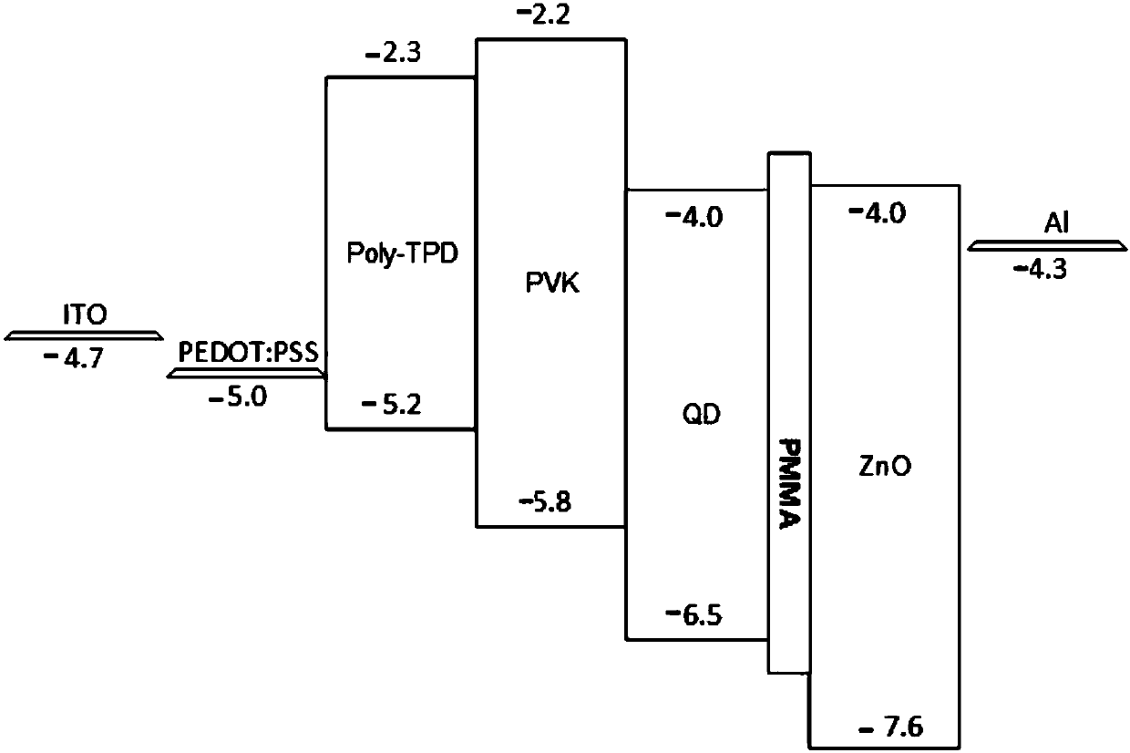
[0113] Figure 6 The energy level schematic diagram of the quantum dot light-emitting diode ...
PUM
| Property | Measurement | Unit |
|---|---|---|
| Thickness | aaaaa | aaaaa |
Abstract
Description
Claims
Application Information
 - R&D
- Intellectual Property
- Life Sciences
- Materials
- Tech Scout
- Unparalleled Data Quality
- Higher Quality Content
- 60% Fewer Hallucinations
Browse by: Latest US Patents, China's latest patents, Technical Efficacy Thesaurus, Application Domain, Technology Topic, Popular Technical Reports.
© 2025 PatSnap. All rights reserved.Legal|Privacy policy|Modern Slavery Act Transparency Statement|Sitemap|About US| Contact US: help@patsnap.com