Electrooptical modulator

An electro-optic modulator and phase modulation technology, which is applied in the fields of instruments, optics, nonlinear optics, etc., can solve the problems of low maturity, less commercial use, and large size, and achieve the goal of increasing modulation bandwidth, improving modulation efficiency, and reducing insertion loss Effect

Inactive Publication Date: 2019-09-13
INST OF SEMICONDUCTORS - CHINESE ACAD OF SCI
View PDF4 Cites 8 Cited by
  • Summary
  • Abstract
  • Description
  • Claims
  • Application Information

AI Technical Summary

Problems solved by technology

Among them, LiNbO 3 The modulator is the most mature electro-optic modulator with large bandwidth and good reliability, but it is large in size and difficult to integrate with lasers and detectors; the InP modulator is easy to

Method used


Image

  • Electrooptical modulator
  • Electrooptical modulator
  • Electrooptical modulator

Examples


Embodiment

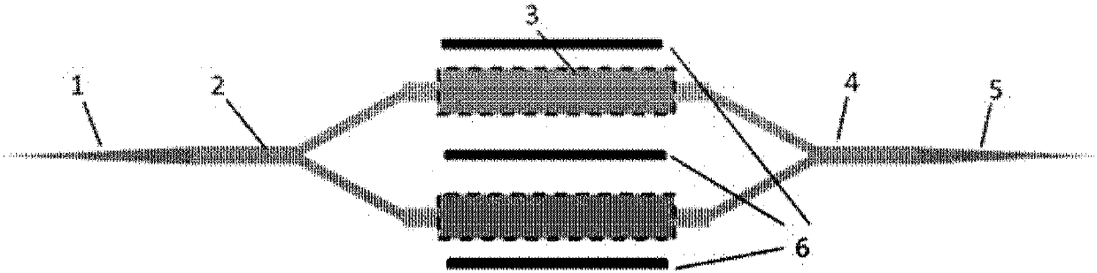
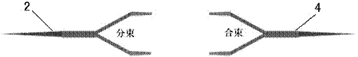
[0048] like figure 1 As shown, this embodiment provides a high-performance electro-optic modulator of a mixed material system with large bandwidth, low half-wave voltage, and low insertion loss. The electro-optic modulator includes a first speckle converter 1, a Y-branch splitting optical waveguide 2, a hybrid integrated phase modulation arm 3, a Y-branch combining optical waveguide 4, a second speckle converter 5 and a traveling wave electrode 6. The electro-optic modulator is formed on a silicon dioxide layer 8 on a silicon substrate 7, wherein:

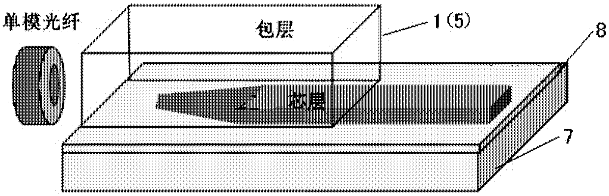
[0049] like figure 2 As shown, the first and second mode spot converters 1 and 5 are composed of core silicon waveguide and cladding silicon dioxide. The core layer is etched to form a horizontal wedge-shaped structure, and the size of the wedge-shaped end face is small to a certain extent. It will diverge to the cladding transmission, thereby expanding the optical mode field, matching it with the optical mode field of the singl...


PUM


Abstract

The invention discloses an electrooptical modulator which comprises mode spot converters, Y-branch beam splitting optical waveguide, Y-branch beam combining optical waveguide, hybrid integration phasemodulation arms and travelling wave electrodes, wherein the mode spot converters are used for reducing mode field mismatching of single-mode optical fibers and the modulator and realizing high-efficiency coupling of optical fields of the single-mode optical fibers and the modulator; the Y-branch beam splitting optical waveguide is used for splitting a laser beam to form beam splitting laser; thehybrid integration phase modulation arms are used for transmitting laser, converting optical mode fields and realizing high-efficiency modulation of an electrical signal to an optical signal; the travelling wave electrodes facilitate realization of speed matching of optical wave and microwave, and further improve the band width of the modulator; and the Y-branch beam combining optical waveguide isused for combining the modulated beam splitting laser into a laser beam. The modulator integrates the mode spot converters, so that the coupling loss of the optical fields from the optical fibers tothe modulator is greatly reduced; and the insertion loss of the modulator is reduced. The modulator can obviously improve the electrooptical modulation efficiency, so that the half-wave voltage of themodulator can be reduced.

Description

technical field [0001] The invention belongs to the technical field of semiconductor integration, and more specifically relates to a hybrid integrated high-performance electro-optical modulator. Background technique [0002] In recent years, radar and electronic countermeasures, wireless communication and other information systems are developing rapidly in the direction of broadband, integration and miniaturization. These information systems have strict requirements on the analog optical link. The modulator is the core device in the analog optical link. It needs to have high bandwidth, low half-wave voltage, low insertion loss, small size and high linearity. [0003] Many institutions at home and abroad have conducted in-depth explorations on the development of high-performance modulators, and have achieved fruitful progress and results. According to the classification of material system, electro-optic modulators are mainly divided into lithium niobate (LiNbO 3 ) modulator...

Claims


Application Information

Patent Timeline
IPC IPC(8): G02F1/01G02F1/035
CPCG02F1/011G02F1/035G02F1/0113
Inventor 李金野刘建国于丽娟邹灿文于海洋
Owner INST OF SEMICONDUCTORS - CHINESE ACAD OF SCI
Why Eureka
Try Eureka