

Silicon wafer etching method, method for preparing antireflective texture surface on silicon wafer surface and method for etching specific patterns on silicon wafer surface
A silicon wafer surface and silicon wafer technology, applied in the field of semiconductor etching, can solve the problems of high process cost, cumbersome process, metal pollution on the silicon wafer surface, etc.
- Summary
- Abstract
- Description
- Claims
- Application Information
AI Technical Summary
Problems solved by technology
Method used
Image

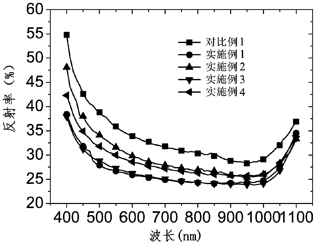
Examples
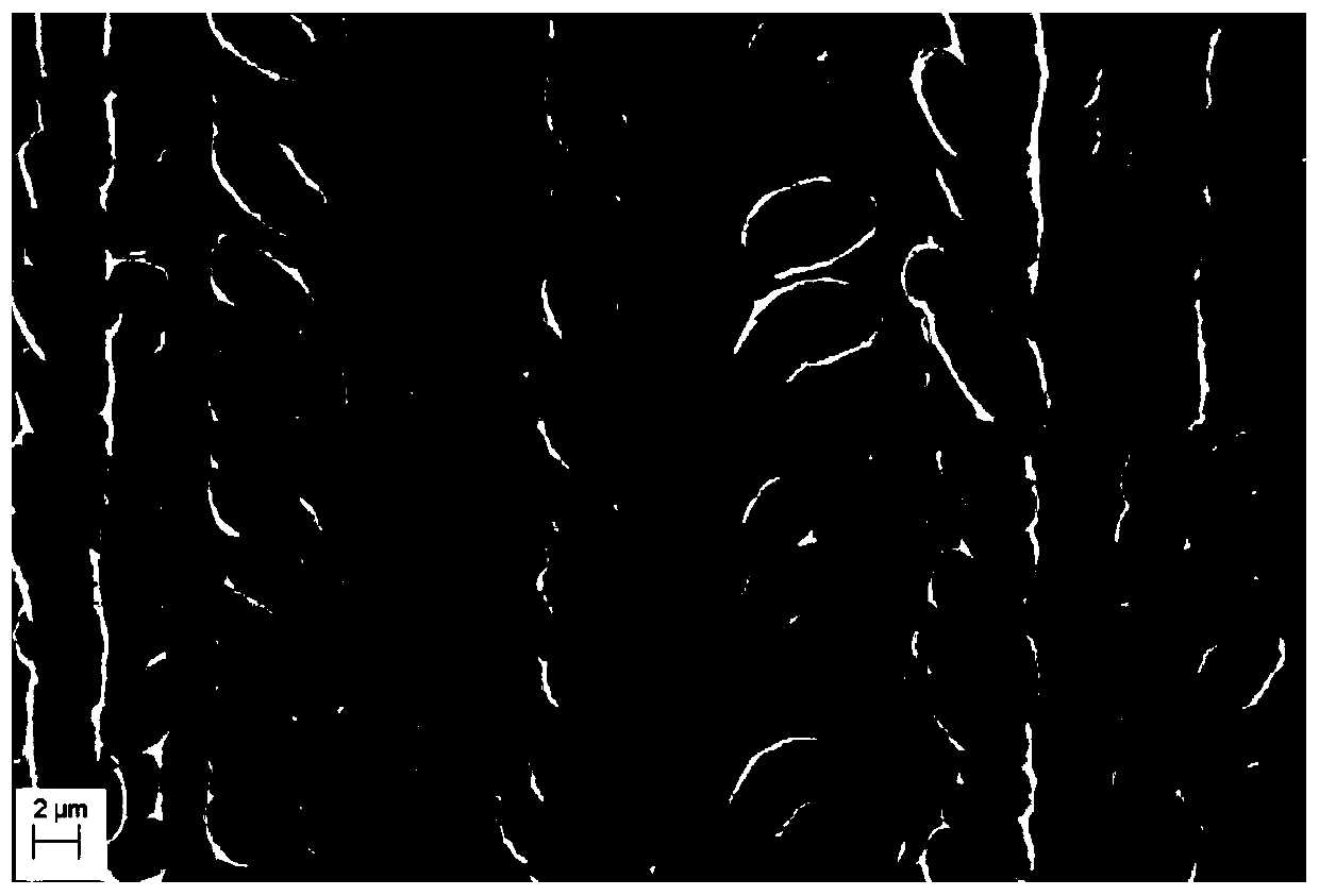
Embodiment 1
[0049] (1) MnO with a particle size of less than 10 μm 2 The powder particles are mixed with the mixed acid solution of HF and HCl to obtain a suspension; the concentration of HCl is 15.4mol / L, the concentration of HF is 14.3mol / L, MnO 2 The concentration is 8.3g / L;
[0050] (2) At room temperature, place diamond wire-cut polysilicon slices horizontally into the bottom of the suspension to make the MnO 2 The particles naturally settled on the silicon wafer, and were removed after etching for 30 minutes;
[0051] (3) Dip the etched silicon wafer into an alkaline washing solution, and perform an alkaline washing at room temperature for 15 s, and the alkaline washing solution is an aqueous NaOH solution with a concentration of 5.0 wt.%.
[0052] (4) At room temperature, immerse the silicon chip after the alkali cleaning in the pickling solution, pickle for 2min, and the pickling solution is a mixed aqueous solution of HF and HCl, wherein the concentration of HF is 2.8mol / L, and...
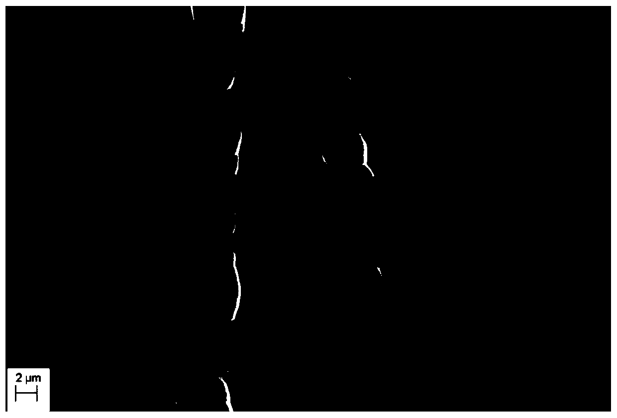
Embodiment 2
[0055] (1) MnO with a particle size of less than 10 μm 2 The powder particles are mixed with the mixed acid solution of HF and HCl to obtain a suspension; the concentration of HCl is 15.4mol / L, the concentration of HF is 14.3mol / L, MnO 2 The concentration is 16.7g / L;
[0056] (2) Carry out standard RCA cleaning to the polysilicon wafer cut by diamond wire;
[0057] (3) At room temperature, place the diamond wire-cut polysilicon slices cleaned in step (2) horizontally into the bottom of the suspension, so that the MnO 2 The particles naturally settled on the silicon wafer, and were removed after etching for 8 minutes;
[0058] (4) Dip the etched silicon wafer into an alkaline washing solution, and perform an alkaline washing at room temperature for 15 s, and the alkaline washing solution is an aqueous NaOH solution with a concentration of 5.0 wt.%.
[0059] (5) At room temperature, immerse the silicon chip after the alkali cleaning in the pickling solution, pickle for 2min, ...
Embodiment 3
[0062] (1) MnO with a particle size of less than 10 μm 2 The powder particles are mixed with the mixed acid solution of HF and HCl to obtain a suspension; the concentration of HCl is 19.8mol / L, the concentration of HF is 22.6mol / L, MnO 2 The concentration is 33.3g / L;
[0063] (2) Carry out the APM (SC-1) and HPM (SC-2) cleaning in the standard RCA cleaning of the polysilicon wafer cut by diamond wire in sequence;
[0064] (3) At room temperature, place the diamond wire-cut polysilicon slices cleaned in step (2) horizontally into the bottom of the suspension, so that the MnO 2 The particles naturally settled on the silicon wafer, and were removed after etching for 10 minutes;
[0065] (4) Dip the etched silicon wafer into an alkaline washing solution, and perform an alkaline washing at room temperature for 15 s, and the alkaline washing solution is an aqueous NaOH solution with a concentration of 5.0 wt.%.
[0066] (5) At room temperature, immerse the silicon chip after the ...
PUM
| Property | Measurement | Unit |
|---|---|---|
| Particle size | aaaaa | aaaaa |
| Concentration | aaaaa | aaaaa |
Abstract
Description
Claims
Application Information