
A method for etching a silicon wafer, a method for preparing an anti-reflection texture on the surface of a silicon wafer, and a method for etching specific patterns on the surface of a silicon wafer

A silicon wafer surface, anti-reflection technology, applied in the direction of final product manufacturing, sustainable manufacturing/processing, semiconductor/solid-state device manufacturing, etc., can solve the problems of high process cost, metal pollution on the surface of silicon wafer, cumbersome process, etc.

Active Publication Date: 2022-03-01
INST OF ELECTRICAL ENG CHINESE ACAD OF SCI
View PDF2 Cites 0 Cited by
  • Summary
  • Abstract
  • Description
  • Claims
  • Application Information

AI Technical Summary

Problems solved by technology

The problem with this technology is that precious metals are needed as catalysts, the process cost is high, and there is metal contamination on the surface of the obtained silicon wafer, which requires subsequent cleaning steps, and the process is cumbersome

Method used

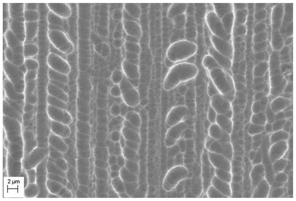
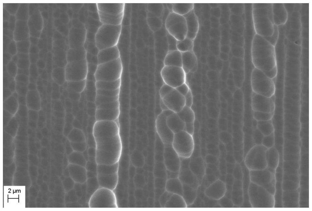
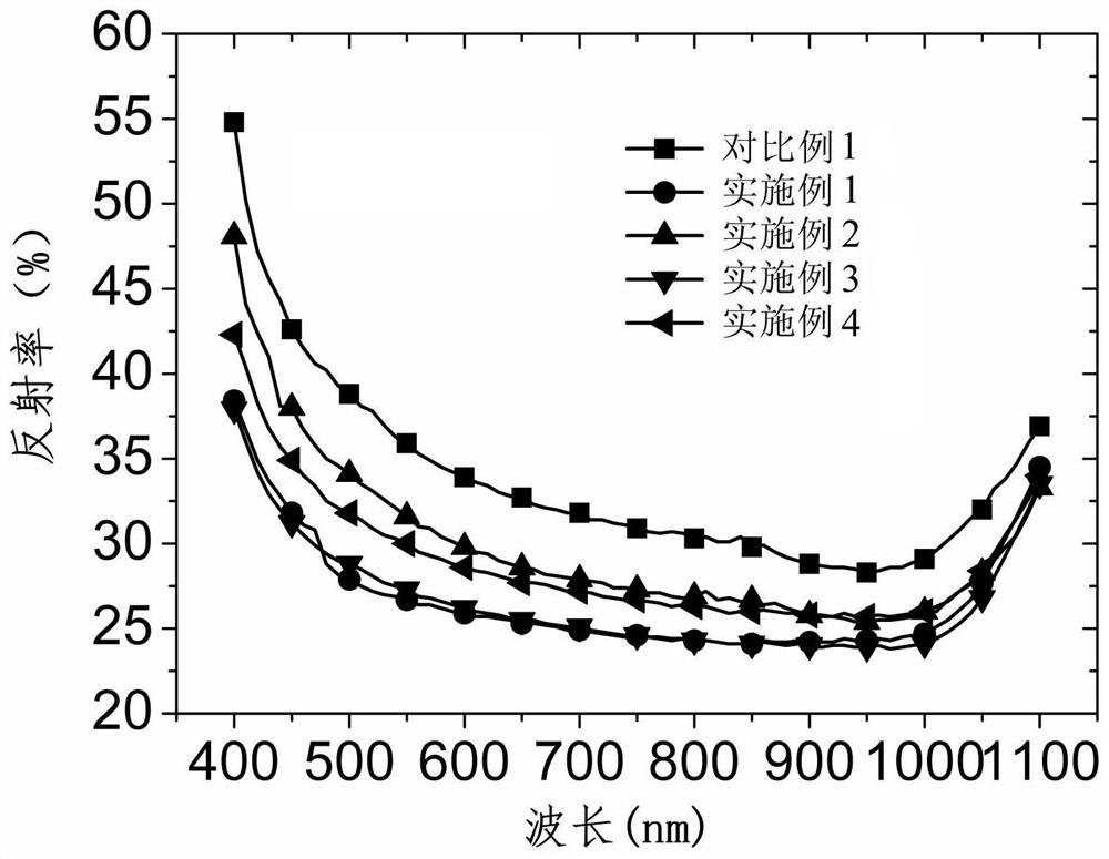

Image

  • A method for etching a silicon wafer, a method for preparing an anti-reflection texture on the surface of a silicon wafer, and a method for etching specific patterns on the surface of a silicon wafer
  • A method for etching a silicon wafer, a method for preparing an anti-reflection texture on the surface of a silicon wafer, and a method for etching specific patterns on the surface of a silicon wafer
  • A method for etching a silicon wafer, a method for preparing an anti-reflection texture on the surface of a silicon wafer, and a method for etching specific patterns on the surface of a silicon wafer

Examples


Embodiment 1

[0049] (1) MnO with a particle size of less than 10 μm 2 The powder particles are mixed with the mixed acid solution of HF and HCl to obtain a suspension; the concentration of HCl is 15.4mol / L, the concentration of HF is 14.3mol / L, MnO 2 The concentration is 8.3g / L;

[0050] (2) At room temperature, place diamond wire-cut polysilicon slices horizontally into the bottom of the suspension to make the MnO 2 The particles naturally settled on the silicon wafer, and were removed after etching for 30 minutes;

[0051] (3) Dip the etched silicon wafer into an alkaline washing solution, and perform an alkaline washing at room temperature for 15 s, and the alkaline washing solution is an aqueous NaOH solution with a concentration of 5.0 wt.%.

[0052] (4) At room temperature, immerse the silicon chip after the alkali cleaning in the pickling solution, pickle for 2min, and the pickling solution is a mixed aqueous solution of HF and HCl, wherein the concentration of HF is 2.8mol / L, and...

Embodiment 2

[0055] (1) MnO with a particle size of less than 10 μm 2 The powder particles are mixed with the mixed acid solution of HF and HCl to obtain a suspension; the concentration of HCl is 15.4mol / L, the concentration of HF is 14.3mol / L, MnO 2 The concentration is 16.7g / L;

[0056] (2) Carry out standard RCA cleaning to the polysilicon wafer cut by diamond wire;

[0057] (3) At room temperature, place the diamond wire-cut polysilicon slices cleaned in step (2) horizontally into the bottom of the suspension, so that the MnO 2 The particles naturally settled on the silicon wafer, and were removed after etching for 8 minutes;

[0058] (4) Dip the etched silicon wafer into an alkaline washing solution, and perform an alkaline washing at room temperature for 15 s, and the alkaline washing solution is an aqueous NaOH solution with a concentration of 5.0 wt.%.

[0059] (5) At room temperature, immerse the silicon chip after the alkali cleaning in the pickling solution, pickle for 2min, ...

Embodiment 3

[0062] (1) MnO with a particle size of less than 10 μm 2 The powder particles are mixed with the mixed acid solution of HF and HCl to obtain a suspension; the concentration of HCl is 19.8mol / L, the concentration of HF is 22.6mol / L, MnO 2 The concentration is 33.3g / L;

[0063] (2) Carry out the APM (SC-1) and HPM (SC-2) cleaning in the standard RCA cleaning of the polysilicon wafer cut by diamond wire in sequence;

[0064] (3) At room temperature, place the diamond wire-cut polysilicon slices cleaned in step (2) horizontally into the bottom of the suspension, so that the MnO 2 The particles naturally settled on the silicon wafer, and were removed after etching for 10 minutes;

[0065] (4) Dip the etched silicon wafer into an alkaline washing solution, and perform an alkaline washing at room temperature for 15 s, and the alkaline washing solution is an aqueous NaOH solution with a concentration of 5.0 wt.%.

[0066] (5) At room temperature, immerse the silicon chip after the ...


PUM

PropertyMeasurementUnit
particle diameteraaaaaaaaaa
concentrationaaaaaaaaaa

Abstract

The invention provides a method for etching a silicon chip, a method for preparing an anti-reflection textured surface on the surface of a silicon chip and a method for etching a specific pattern on the surface of a silicon chip, belonging to the technical field of semiconductor etching. The present invention uses solid MnO 2 As an oxidizing agent, while HF and other non-oxidizing acids are used to provide solid MnO that can strengthen 2 Oxidizing acidic environment, in acidic environment, solid MnO 2 Shows oxidation, and silicon can be oxidized in contact with silicon wafers, resulting in SiO 2 Etched by HF acid, exposing new silicon surface and solid MnO 2 Contact, continue to be oxidized, as the reaction proceeds, between the silicon wafer and the solid MnO 2 The location of the contact forms an etched structure, the solid MnO 2 is eventually reduced to soluble Mn 2+ ion. The method can be used for fixed-point etching on the surface of the silicon wafer where etching is required, and can also be used for the preparation of an anti-reflection textured surface on the surface of a polycrystalline silicon wafer. The textured surface with low reflectivity can be obtained without using noble metals or nitric acid.

Description

technical field [0001] The invention relates to the technical field of semiconductor etching, in particular to a method for etching a silicon chip, a method for preparing an anti-reflection texture on the surface of a silicon chip and a method for etching a specific pattern on the surface of a silicon chip. Background technique [0002] Etching silicon wafers to form patterned or randomly distributed micro-nano structures is a necessary step in the manufacture of many semiconductor devices. The techniques for etching silicon wafers are mainly divided into dry etching and wet etching. [0003] Dry etching mainly utilizes reactive gas or / and plasma to etch through chemical or / and physical action. A representative method for dry etching of silicon wafers is reactive ion etching (RIE: Reactive Ion Etching), which is usually a combination of reactive gases containing halogen atoms (such as CF 4 / O 2 , SF 6 / O 2 etc.) into the plasma electric field, combined with the chemical...

Claims


Application Information

Patent Timeline
Patent Type & Authority Patents(China)
IPC IPC(8): H01L21/306H01L31/18H01L31/0236
CPCH01L21/30608H01L31/1804H01L31/02363Y02P70/50
Inventor 刘欢赵雷王文静
Owner INST OF ELECTRICAL ENG CHINESE ACAD OF SCI
Learn More