Free-standing ultrafine nanocrystalline diamond thick film
A diamond thick film, ultra-fine nanotechnology, applied in the field of diamond materials, can solve problems such as large grain size, increased processing procedures and costs, and restrictions on the large-scale industrial application of micron diamonds
- Summary
- Abstract
- Description
- Claims
- Application Information
AI Technical Summary
Problems solved by technology
Method used
Image

Examples
Embodiment 1
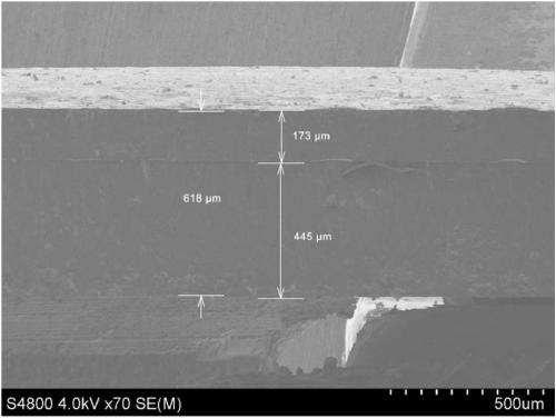
[0056] A silicon (100) surface with a diameter of 50-100 millimeters and a thickness of 500-3000 micrometers is used for chemical vapor deposition of an ultrafine nanocrystalline diamond thick film. Before deposition, in order to increase the nucleation density of diamond to grow ultrafine nanocrystalline diamond, it is necessary to grind the silicon wafer with ultrafine nanocrystalline diamond powder to form many nanogrooves on the surface of the silicon wafer to promote the nucleation of diamond. The particle size of ultra-fine nanocrystalline diamond powder is 5-15 nanometers, and the silicon wafer is ground by manual grinding. After the ground silicon wafer is ultrasonically cleaned with deionized water, it is ultrasonicated in an alcohol suspension containing ultrafine nanocrystalline diamond powder, and seeds are placed on the surface of the silicon wafer, and the ultrasonic time is 5-30 minutes. High-density ultrafine nanocrystalline diamond powder will remain on the su...
Embodiment 2
[0069] Adopt the method for embodiment 1 to prepare self-supporting ultrafine nanocrystalline diamond thick film, difference is: the height of hot wire distance sample is 14 millimeters, growth pressure 1.5kPa, methane concentration 2%, inert gas concentration 10%, growth time 30-1000 hours to complete the growth of ultra-fine nanocrystalline diamond thick film.
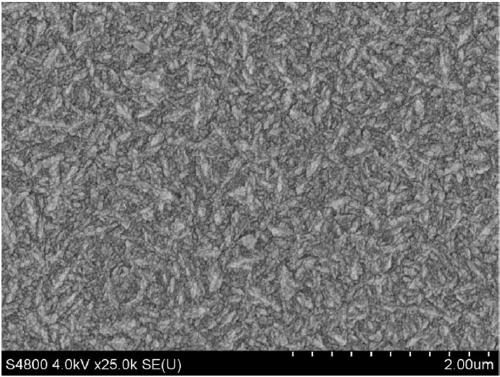
[0070] Figure 8 It is a plane scanning electron micrograph of ultrafine nanocrystalline diamond thick film. From Figure 8 It can be seen from the figure that the crystal grains of the diamond thick film are still ultrafine nanocrystals, and compared with Example 1, the needle-like clusters are more obvious.
[0071] Figure 9 It is ultrafine nanocrystalline diamond thick film Raman spectrum. From Figure 9 It can be seen from the figure that there are 6 Raman peaks of the diamond thick film, at 1134, 1192, 1332, 1350, 1470, 1550cm -1 , is a typical Raman spectrum of nanocrystalline diamond.
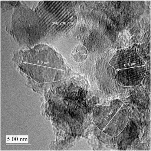
[0072] After test...
Embodiment 3
[0074] Adopt the method for embodiment 1 to prepare self-supporting ultrafine nanocrystalline diamond thick film, difference is: the height of hot wire distance sample is 15 millimeters, growth pressure 1.5kPa, methane concentration 2%, inert gas concentration 10%, growth time 30-1000 hours to complete the growth of ultra-fine nanocrystalline diamond thick film.
[0075] Figure 10 It is a plane scanning electron micrograph of ultrafine nanocrystalline diamond thick film. From Figure 10 It can be seen from the figure that the crystal grains of the diamond thick film are still ultrafine nanocrystals. Compared with Example 1, the distribution of diamond grains is no longer needle-like clusters.
[0076] Figure 11 It is ultrafine nanocrystalline diamond thick film Raman spectrum. From Figure 11 It can be seen from the figure that there are 6 Raman peaks of the diamond thick film, at 1134, 1192, 1332, 1350, 1470, 1550cm -1 , is a typical Raman spectrum of nanocrystalline ...
PUM
| Property | Measurement | Unit |
|---|---|---|
| thickness | aaaaa | aaaaa |
| size | aaaaa | aaaaa |
| diameter | aaaaa | aaaaa |
Abstract
Description
Claims
Application Information
 - R&D
- Intellectual Property
- Life Sciences
- Materials
- Tech Scout
- Unparalleled Data Quality
- Higher Quality Content
- 60% Fewer Hallucinations
Browse by: Latest US Patents, China's latest patents, Technical Efficacy Thesaurus, Application Domain, Technology Topic, Popular Technical Reports.
© 2025 PatSnap. All rights reserved.Legal|Privacy policy|Modern Slavery Act Transparency Statement|Sitemap|About US| Contact US: help@patsnap.com