AlGaN/GaN heterojunction Schottky diode device based on P-GaN cap layer and floating metal ring

A technology of Schottky diodes and metal rings, applied in the direction of diodes, semiconductor/solid-state device manufacturing, semiconductor devices, etc., can solve the problems of slow lateral potential changes, influence of forward characteristics, increase of series resistance, etc., and achieve reverse leakage Effects of leakage current suppression, defect avoidance, and breakdown voltage improvement

Active Publication Date: 2019-10-22
XIDIAN UNIV
View PDF5 Cites 4 Cited by
  • Summary
  • Abstract
  • Description
  • Claims
  • Application Information

AI Technical Summary

Problems solved by technology

The floating metal ring structure is to deposit and form several floating Schottky metal electrodes between the cathode and cathode metals. When a reverse bias is applied, the space charge region of the cathode metal will increase with the increase of the reverse bias. Widening, when extending to the position of the floating metal ring, due to the equipotential effect of the floating metal ring, the lateral potential here changes slowly, and the corresponding electric field peak value in the Schottky contact area decreases, improving the electric field concentration effect and improving Reverse breakdown voltage, while the floating metal ring structure will not introduce other parasitic capacitance, but, due to the depletion effect of the floating metal ring Schottky metal, the series resistance will increase, which will have some impact on the forward characteristics

Method used


Image

  • AlGaN/GaN heterojunction Schottky diode device based on P-GaN cap layer and floating metal ring
  • AlGaN/GaN heterojunction Schottky diode device based on P-GaN cap layer and floating metal ring
  • AlGaN/GaN heterojunction Schottky diode device based on P-GaN cap layer and floating metal ring

Examples


Embodiment 1

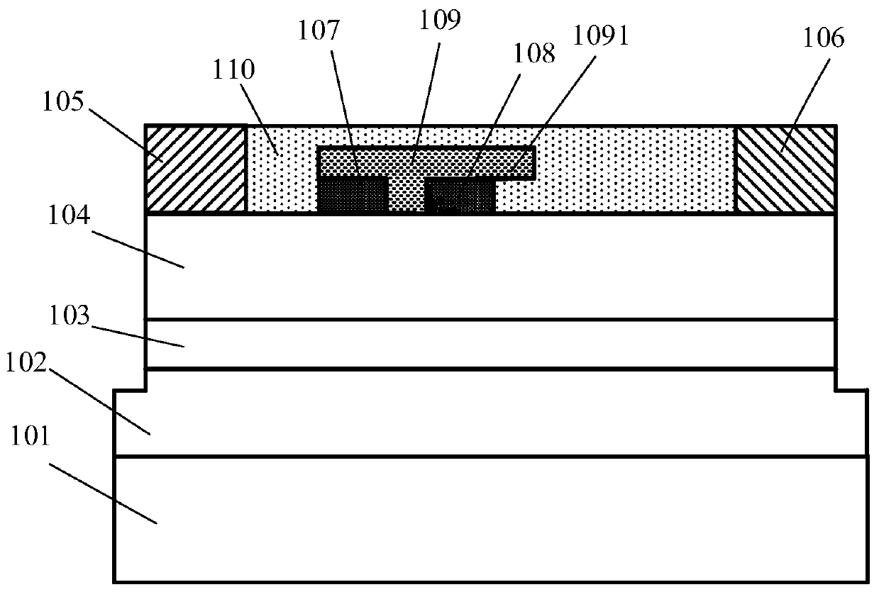
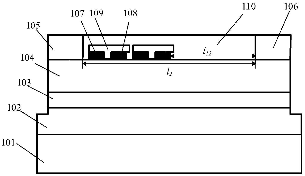
[0036] See figure 1 , figure 1It is a schematic structural diagram of an AlGaN / GaN heterojunction Schottky diode device based on a P-GaN cap layer and a floating metal ring provided by an embodiment of the present invention. The AlGaN / GaN heterojunction Schottky diode device includes a substrate 101, a GaN buffer layer 102, a channel layer 103, an AlGaN barrier layer 104, and a passivation layer 110 sequentially arranged on the substrate 101, wherein the AlGaN An anode 105 and a cathode 106 are respectively provided on opposite sides of the upper surface of the barrier layer 104, and at least one composite structure is provided on the AlGaN barrier layer 104 between the anode 105 and the cathode 106, and the composite structure includes a first P-type GaN The cap layer 107, the second P-type GaN cap layer 108 and the floating metal ring 109; the first P-type GaN cap layer 107 and the second P-type GaN cap layer 108 are arranged on the AlGaN barrier layer 104 at intervals, and...

Embodiment 2

[0051] On the basis of the above embodiments, this embodiment provides another AlGaN / GaN heterojunction Schottky diode device based on a P-GaN cap layer and a floating metal ring.

[0052] As mentioned above, at least one of the combined structures is provided on the AlGaN barrier layer 104 between the anode 105 and the cathode 106, that is to say, a plurality of the above-mentioned composite structures can be provided on the AlGaN barrier layer 104 between the anode 105 and the cathode 106. the combined structure. The main difference between this embodiment and Embodiment 1 is that this embodiment may include multiple combined structures, wherein, along the direction from the anode 105 to the cathode 106, the first P-type GaN cap layer 107 of the first combined structure is located One side close to the anode 105 and spaced apart from the anode 105; the second P-type GaN cap layer 108 of the last combination structure is located on the side close to the cathode 106 and spaced...

Embodiment 3

[0060] On the basis of the above embodiments, this embodiment provides a method for manufacturing an AlGaN / GaN heterojunction Schottky diode device based on a P-GaN cap layer and a floating metal ring. See Figure 7a to Figure 7f , Figure 7a to Figure 7f It is a schematic diagram of the preparation process of an AlGaN / GaN heterojunction Schottky diode device based on a P-GaN cap layer and a floating metal ring provided by an embodiment of the present invention.

[0061] Described preparation method comprises:

[0062] Step 1: using MOCVD (metal organic vapor deposition) process to epitaxially grow the heterojunction.

[0063] 1.1) Select SiC or sapphire substrate, such as Figure 7a shown;

[0064] 1.2) On the SiC or sapphire substrate, grow an intrinsic GaN layer with a thickness of 1 μm;

[0065] 1.3) A 25nm-thick AlGaN barrier layer is grown on the intrinsic GaN layer, wherein the composition of Al is 20%, and a two-dimensional electron gas is formed at the contact po...


PUM


Abstract

The invention discloses an AlGaN / GaN heterojunction Schottky diode device based on a P-GaN cap layer and floating metal ring composite structure. The AlGaN / GaN heterojunction Schottky diode device comprises a substrate, and a GaN buffer layer, a channel layer, an AlGaN barrier layer and a passivation layer which are sequentially arranged on the substrate, an anode and a cathode are respectively arranged on two opposite sides of the upper surface of the AlGaN barrier layer, at least one combined structure is arranged on the AlGaN barrier layer between the anode and the cathode, and each combined structure comprises a first P-type GaN cap layer, a second P-type GaN cap layer and a floating metal ring; the first P-type GaN cap layer and the second P-type GaN cap layer are arranged on the AlGaN barrier layer at intervals, and the floating metal ring covers the upper surfaces of the first P-type GaN cap layer and the second P-type GaN cap layer and the AlGaN barrier layer between the firstP-type GaN cap layer and the second P-type GaN cap layer. The device adopts a structure combining the P-GaN cap layer and the floating metal ring, inhibits the electric field concentration effect, weakens the peak electric field, and ensures that the electric field is distributed more uniformly in the transverse direction, thereby reversely improving the breakdown voltage.

Description

technical field [0001] The invention belongs to the technical field of semiconductor devices, in particular to an AlGaN / GaN heterojunction Schottky diode device based on a P-GaN cap layer and a floating metal ring. Background technique [0002] With the development of microelectronics technology, the third-generation wide-bandgap compound semiconductor materials represented by GaN rely on high critical breakdown field strength, high thermal conductivity, high saturation electron velocity, and good high temperature resistance and radiation resistance. It shows great potential in power devices. Theoretically, the critical breakdown electric field strength of Si is 0.6MV / cm, while the critical breakdown electric field strength of GaN is more than 5 times that of Si, so under the same area, GaN can withstand higher voltage and obtain greater power . [0003] At present, GaN-based Schottky diodes are mainly divided into: GaN matrix material Schottky diodes and AlGaN / GaN heteroj...

Claims


Application Information

Patent Timeline
Patent Type & Authority Applications(China)
IPC IPC(8): H01L29/872H01L29/40H01L29/205H01L29/20H01L21/329
CPCH01L29/2003H01L29/205H01L29/407H01L29/66212H01L29/66219H01L29/872
Inventor 王冲刘凯马晓华郑雪峰何云龙郝跃
Owner XIDIAN UNIV
Why Eureka
Try Eureka